Wiring Pattern Inspection Method and Inspection Apparatus for Flexible Printed Wiring Board

a flexible printed wiring and inspection method technology, applied in the direction of dielectric characteristics, inspection/indentification of circuits, instruments, etc., can solve the problem that the ability to detect short-circuit defects of the method is inferior, and the determination of the quality of the wiring pattern cannot be appropriately performed with either method alone, so as to achieve the detection of the quality of the wiring pattern, simple structure, and the effect of increasing the measurement tim

Inactive Publication Date: 2009-06-18
MITSUI MINING & SMELTING CO LTD
View PDF2 Cites 13 Cited by
  • Summary
  • Abstract
  • Description
  • Claims
  • Application Information

AI Technical Summary

Benefits of technology

[0032]According to a wiring pattern inspection method and an inspection apparatus for a flexible printed wiring board of the present invention, by emitting illumination light from a front surface side of the flexible printed wiring board while providing a reflection member whose surface is mirrored on a rear surface side, light transmitted at a light permeable insulating film part having no wiring pattern is reflected at a reflection member, and returns to the front surface side after transmitted through the light permeable insulating film as indirect transmission light. Accordingly, by emitting the illumination light from the front surface side of the flexible printed wiring board while providing the reflection member on the rear surface side of the flexible printed wiring board such that a reflection method becomes main and a transmission method becomes subordinate, and imaging a wiring pattern image of an inspection part on the front surface side, it becomes possible to determine the quality of a wiring pattern taking advantage of the reflection method. Further, by utilizing the indirect transmission light, defects of a short-circuiting type on the light permeable insulating film that are difficult to be detected with the reflection method can be detected simultaneously as darker defects than a base part of the light permeable insulating film, thus providing a bias effect. It becomes possible to detect the quality of a wiring pattern with a simple structure, without increasing the measurement time, without increasing the size and the cost of an inspection apparatus, and without requiring a transmission light source.
[0033]According to the wiring pattern inspection method and the inspection apparatus according to the present invention, by using a drum whose surface is mirrored as the reflection member, a wiring pattern image can be imaged by an imaging unit without defocus at an inspection part, and a favorable inspection becomes possible.
[0034]According to the wiring pattern inspection method and the inspection apparatus according to the present invention, by using a line sensor as the imaging unit, it becomes possible to perform inspection by imaging successively an inspection part while carrying the flexible printed wiring board successively at a predetermined speed without temporarily stopping the flexible printed wiring board, and the measurement tact can be improved.
[0035]According to the wiring pattern inspection method and the inspection apparatus according to the present invention, by using reddish illumination having a good transmittance through the light permeable insulating film, a sufficient light amount for providing a bias effect can be obtained as indirect transmission light reflected from the reflection member, and it becomes possible to make defects of a short-circuiting type on the light permeable insulating film noticeable as dark defects.

Problems solved by technology

However, the reflection method and the transmission method have advantages and disadvantages, and it is known that determination of the quality of a wiring pattern cannot be appropriately performed with either of the methods singly.
In the reflection method, when the wiring pattern becomes finely pitched due to narrow lines and high densification, spaces between the wiring patterns become like bottoms of valleys, and even if there is short-circuiting between the wiring pitches, light is rarely reflected; therefore, the method is inferior in the ability to detect defects of short-circuiting, particularly short-circuiting on the surface of the light permeable insulating film.
On the other hand, in the transmission method, a bottom part of the wiring pattern is inspected, and the method has an advantage that it has a high ability to detect defects of short-circuiting; however, it has an disadvantage that defects on the surface side such as top notches cannot be detected because the surface state of the wiring pattern cannot be observed.

Method used


Image

  • Wiring Pattern Inspection Method and Inspection Apparatus for Flexible Printed Wiring Board
  • Wiring Pattern Inspection Method and Inspection Apparatus for Flexible Printed Wiring Board
  • Wiring Pattern Inspection Method and Inspection Apparatus for Flexible Printed Wiring Board

Examples


Embodiment Construction

[0051]Taking a film carrier tape for mounting an electronic part as an example of a flexible printed wiring board, a wiring pattern inspection method and an inspection apparatus for the film carrier tape for mounting an electronic part as one of the best modes for carrying out the present invention will be explained with reference to the drawings. Note that the drawings show exaggerated frame formats, and the relationship between the thickness and the width of each part is different from the actual one. The present invention is not limited to the embodiments, and can be modified variously insofar as not deviating from the gist of the present invention.

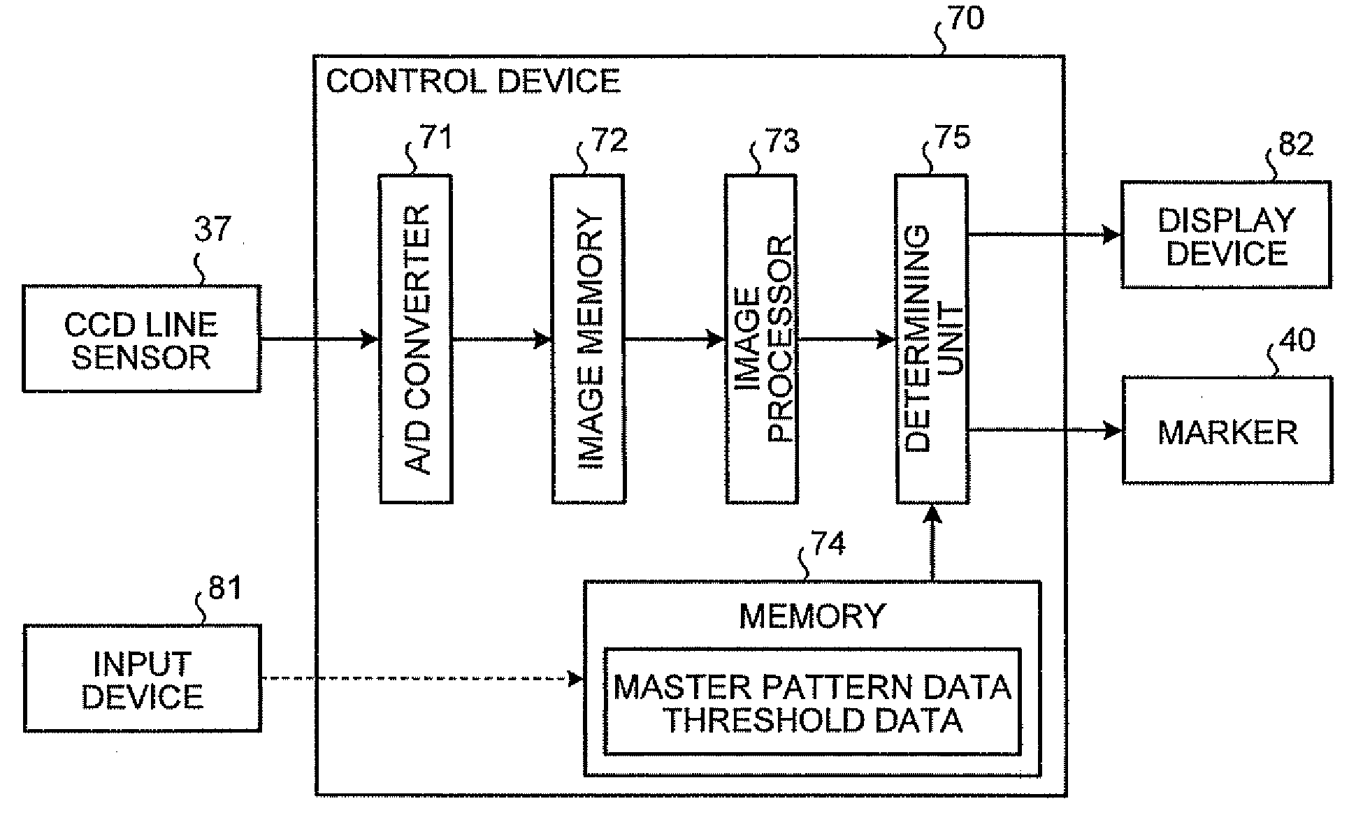
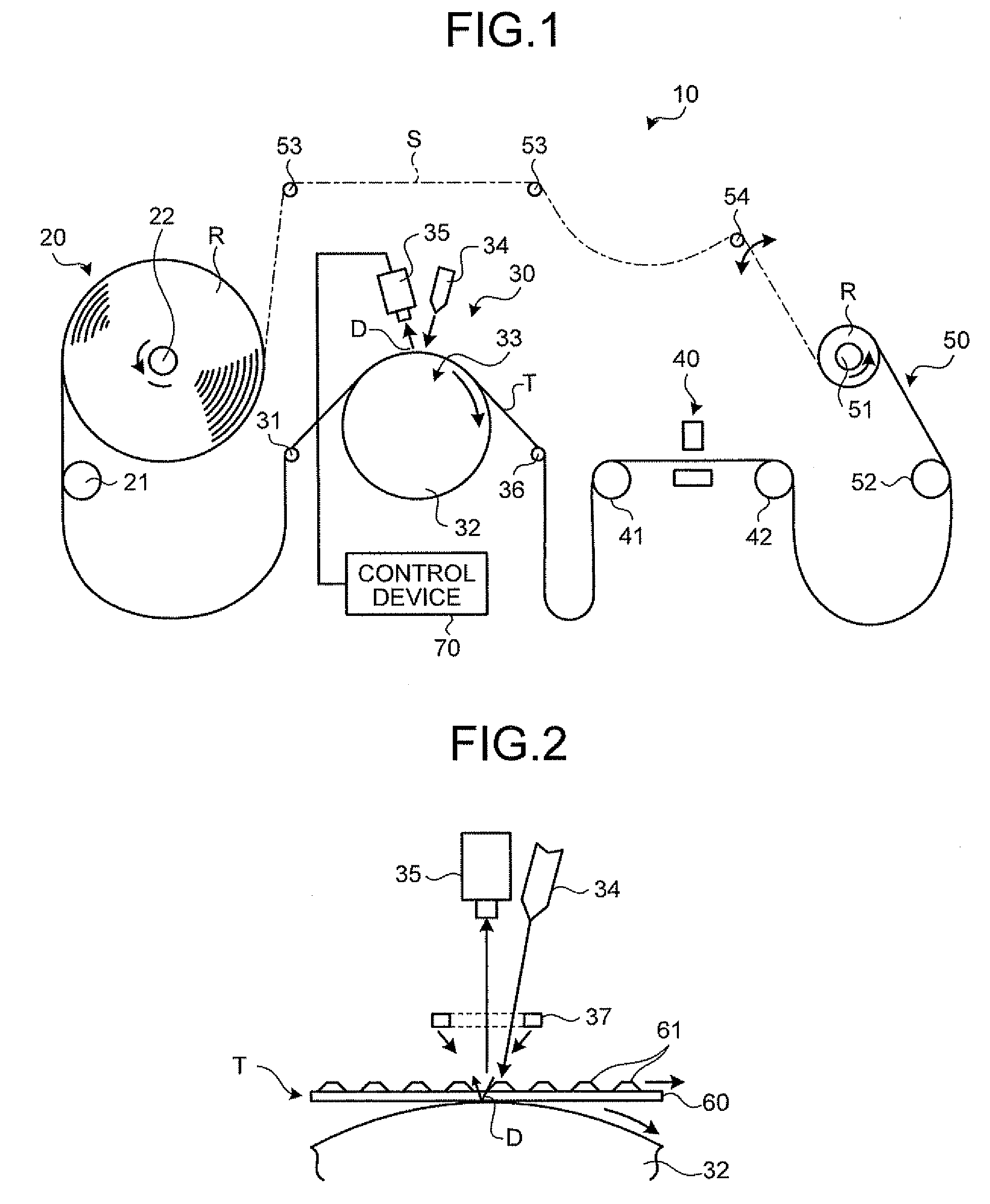
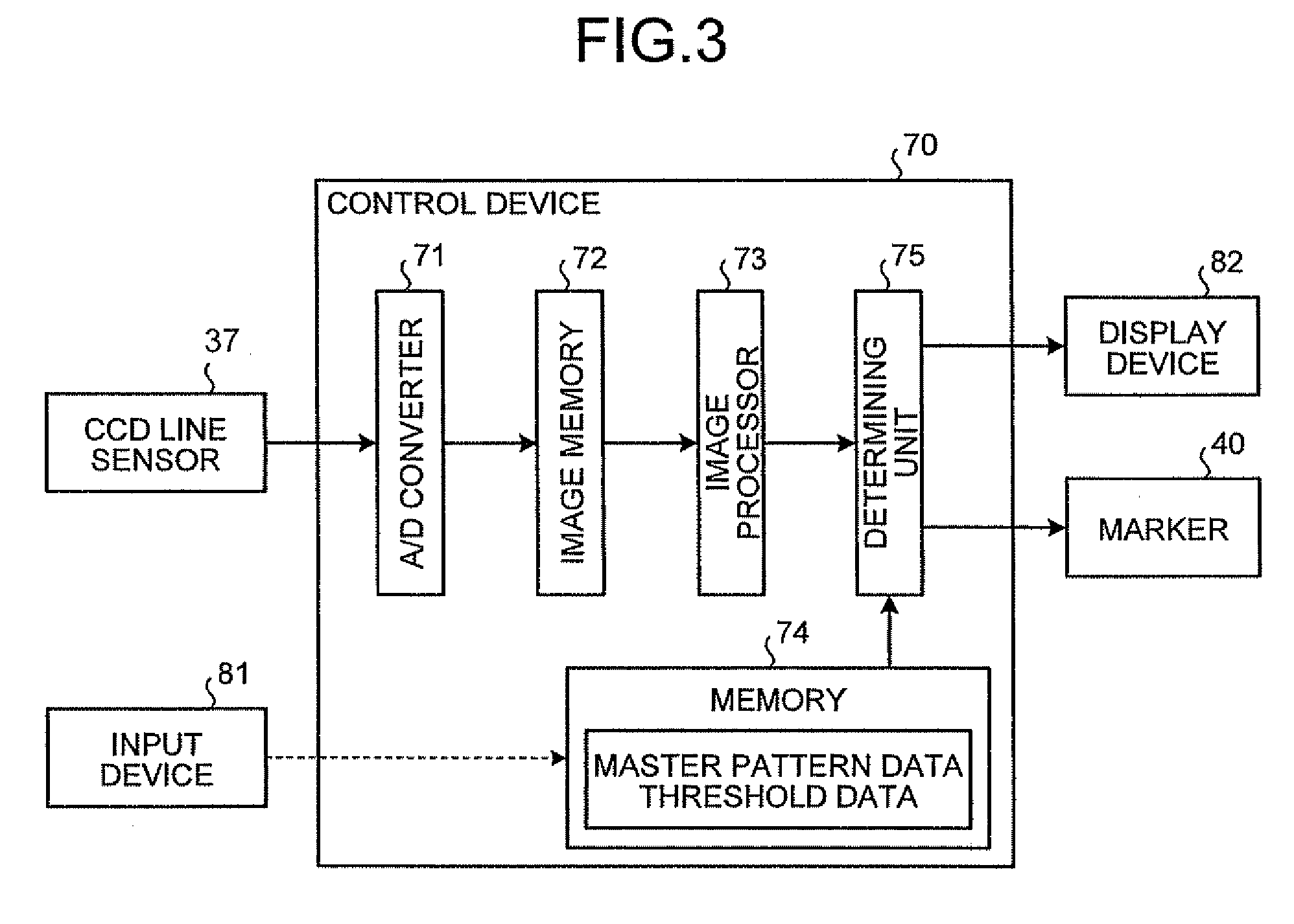
[0052]FIG. 1 is a schematic front view of a structure of a wiring pattern inspection apparatus for performing a wiring pattern inspection method for a film carrier tape for mounting an electronic part according to an embodiment. FIG. 2 is a front view of an enlarged part of a pattern detecting device. A wiring pattern inspection appara...


PUM


Abstract

In a method for inspecting a wiring pattern on a flexible printed wiring board, light is illuminated from a front surface side of the TAB tape T while a drum is provided on the rear surface side of the TAB tape T such that a reflection method becomes main and a transmission method becomes subordinate, and when imaging a wiring pattern image of an inspection part D on the front surface side, it becomes possible to determine the quality of a wiring pattern taking advantage of the reflection method. Furthers by utilizing the indirect transmission light, defects of a short-circuiting type on the light permeable insulating film that are difficult to be detected with the reflection method can be detected as darker defects than the light permeable insulating film by the transmission method.

Description

TECHNICAL FIELD[0001]The present invention relates to a wiring pattern inspection method and an inspection apparatus for a flexible printed wiring board, in particular for a film carrier tape for mounting an electronic part.BACKGROUND ART[0002]With development of the electronics industry, demands for a printed wiring board for mounting electronic parts such as an integrated circuit (IC) chip or a large scale integration (LSI) chip are rapidly increasing. Size reduction, weight reduction, and higher functions of electronic devices are demanded. As a method for mounting these electronic parts, a mounting method in which a flexible printed wiring board, for example a film carrier tape for mounting an electronic part such as a chip on film (COF) tape, a tape carrier package (TCP) tape, a tape ball grid array (BGA) tape, and an application specific integrated circuit (ASIC) tape (hereinafter, simply called a “film carrier tape” or a “tape automated bonding (TAB) tape”) or a flexible prin...

Claims


Application Information

Patent Timeline
Patent Type & Authority Applications(United States)
IPC IPC(8): G06T7/00
CPCG01B11/24H01L2924/0002G01N21/89G01N21/8901G01N21/95684G01N21/958G01N2021/4709G01N2021/4735G01N2021/95638G01R31/2805G01R31/2808H05K1/0269H05K2201/0108G01N21/47H01L2924/00H05K13/06
Inventor NARABAYASHI, TETSUYUKI
Owner MITSUI MINING & SMELTING CO LTD
Why Eureka
Try Eureka