Method of forming a wafer level package

a technology of wafer level and package, applied in the direction of semiconductor devices, semiconductor/solid-state device details, electrical apparatus, etc., can solve the problems of assembly including packages being subject to stress, testing individual chips poses another formidable problem, and terminals moving relative to the conta

Inactive Publication Date: 2009-06-25
TESSERA INC
View PDF6 Cites 3 Cited by
  • Summary
  • Abstract
  • Description
  • Claims
  • Application Information

AI Technical Summary

Benefits of technology

[0014]In accordance with one or more further aspects of the invention, such method may include one or more further additional steps. For example, a second interposer component can be provided which has a second compliant dielectric layer bonded to a second conductive layer. A second pattern of holes can be formed which extend through the second compliant dielectric layer and the second conductive layer corresponding to the pattern of holes through the compliant dielectric layer and the conductive layer. The second compliant dielectric layer can be contacted with the conductive surface so that the second pattern of holes is in an aligned position with the pattern of contacts. The second compliant dielectric layer can be bonded with the conductive surface in the aligned position to unite the second interposer component and the interposer component.
[0015]In accordance with one or more further aspects of the invention, the holes in the second interposer component can be larger than the holes in the interposer component, whereby at least a portion of the conductive surface is exposed.

Problems solved by technology

Testing of individual chips poses another formidable problem with respect to individual handling and interfacing of the test equipment with the relatively delicate unpackaged chips.
Assemblies including packages can suffer from stresses imposed by differential thermal expansion and contraction of the device and the substrate.
Where the terminals of the package are fixed relative to the chip or other device, such as by using solder, these effects tend to cause the terminals to move relative to the contact pads on the circuit board.
This can impose stresses in the solder that connects the terminals to the contact pads on the circuit board.

Method used


Image

  • Method of forming a wafer level package
  • Method of forming a wafer level package
  • Method of forming a wafer level package

Examples


Embodiment Construction

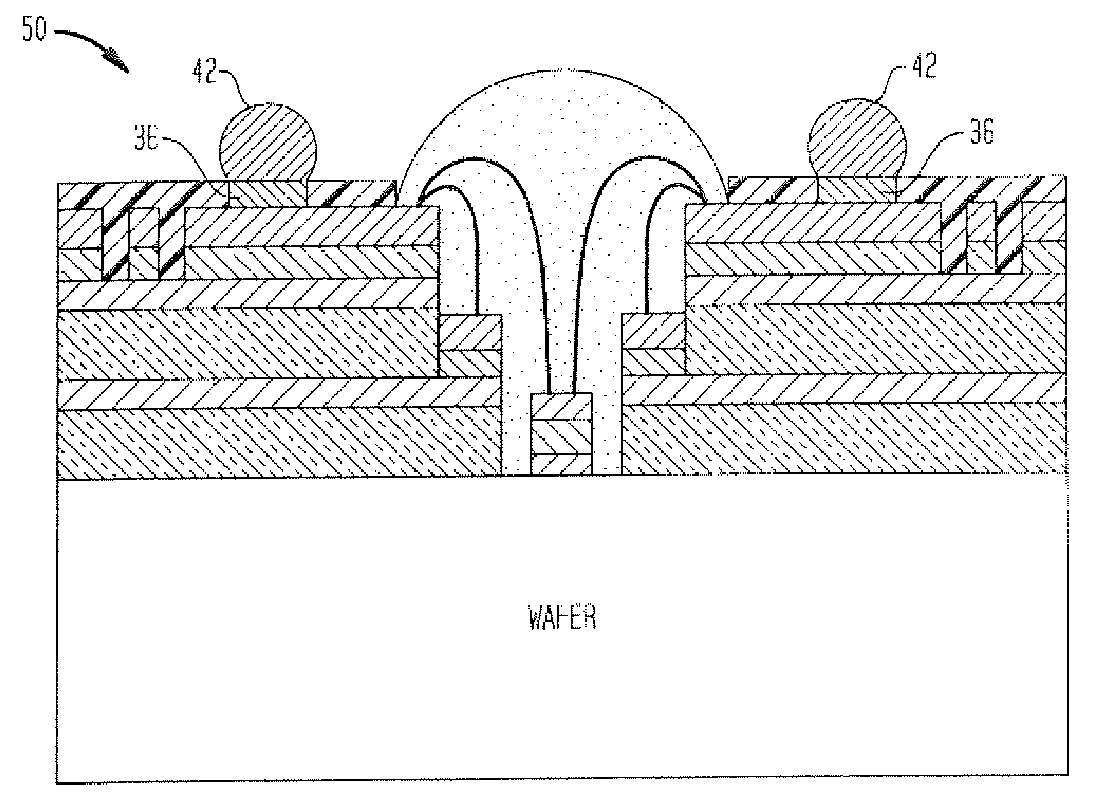
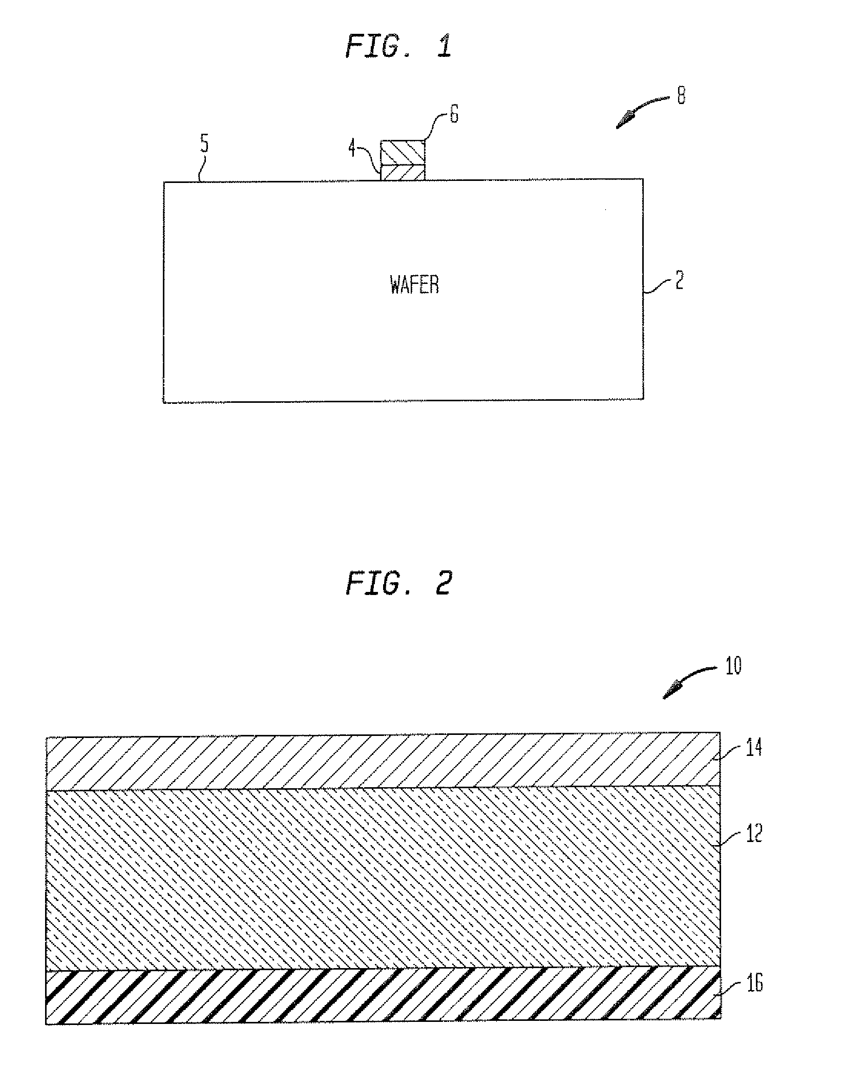
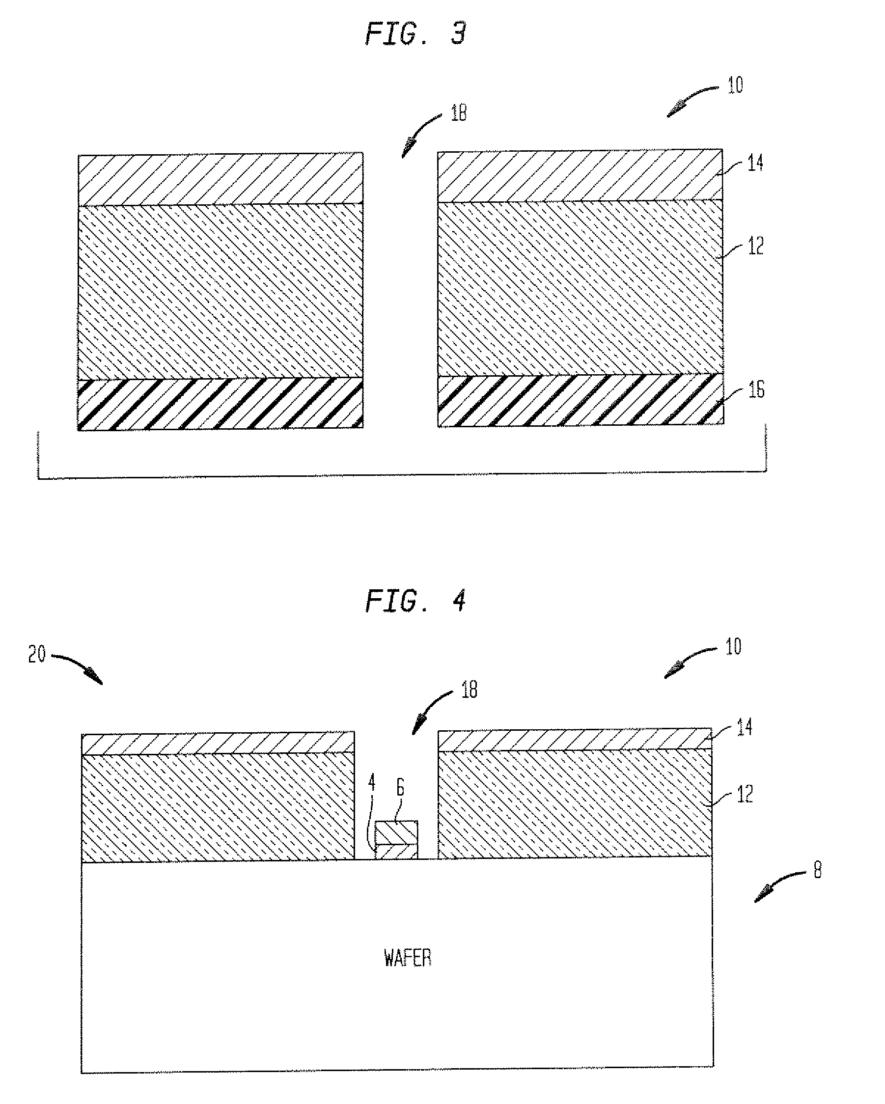
[0027]Referring to FIG. 1, a wafer component 8 includes electrical contacts 4 on an upper surface 5 of a semiconductor wafer 2 containing integrated circuits attached together at dicing lanes (now shown). A contact 4 is typically fashioned of aluminum and is plated with a layer 6 of electro-less nickel in order to make the contact compatible with other metals to be deposited in subsequent steps. Although only one contact is visible in RIG. 1, the wafer contains a pattern of numerous chips and each chip has a pattern of numerous contacts. Once the contacts 4 are plated, the wafer component 8 is prepared for subsequent laminating with protective and signal carrying layers to form a plurality of chip packages at the wafer level for subsequent separation (dicing). Throughout this description, terms such as “upper,”“lower,”“top” and “bottom” do not refer to any gravitational positioning but instead refer to directions in the frame of reference of the components.

[0028]As seen in FIG. 2, t...


PUM


Abstract

A method is provided for forming a microelectronic package at a wafer level. Such method can include providing a semiconductor wafer having a surface with a pattern of electrical contacts thereon. An interposer component can be provided which has a compliant dielectric layer bonded to a conductive layer. A pattern of holes can be formed through the compliant dielectric layer and the conductive layer which corresponds to the pattern of electrical contacts. The compliant dielectric layer can be contacted with the semiconductor wafer surface so that the pattern of holes is in an aligned position with the pattern of contacts and the compliant dielectric layer and the semiconductor wafer surface then bonded in the aligned position to unite the semiconductor wafer and the interposer component to form a wafer level semiconductor package. The wafer level semiconductor package can be diced to form individual semiconductor chip packages.

Description

CROSS-REFERENCE TO RELATED APPLICATIONS[0001]This application claims the benefit of the filing date of U.S. Provisional Patent Application No. 61 / 005,607 filed Dec. 6, 2007, the disclosure of which is hereby incorporated herein by reference.BACKGROUND OF THE INVENTION[0002]The subject matter of the present application relates to microelectronic assemblies and methods for making microelectronic packages and assemblies at a wafer level.[0003]Microelectronic devices such as semiconductor chips typically require many input and output connections to other electronic components. The input and output contacts of a semiconductor chip or other comparable device are generally disposed in grid-like patterns that substantially cover a surface of the device (commonly referred to as an “area array”) or in elongated rows which may extend parallel to and adjacent each edge of the device's front surface, or in the center of the front surface. Typically, devices such as chips must be physically mount...

Claims


Application Information

Patent Timeline
Patent Type & Authority Applications(United States)
IPC IPC(8): H01L21/00
CPCH01L21/4853H01L2924/014H01L23/3114H01L23/3128H01L23/49816H01L24/49H01L2224/48091H01L2224/4824H01L2224/4911H01L2224/49174H01L2924/01005H01L2924/01013H01L2924/01027H01L2924/01028H01L2924/01029H01L2924/01079H01L2924/14H01L2924/15311H01L2924/19107H01L23/13H01L2924/01043H01L2924/01033H01L2924/01006H01L24/48H01L2924/00014H01L2224/45099H01L2224/05599
Inventor HONER, KENNETH ALLENHABA, BELGACEMOVRUTSKY, DAVIDROSENSTEIN, CHARLESGAO, GUILIAN
Owner TESSERA INC
Why Eureka
Try Eureka