Ceramic package, method of manufacturing the same, electronic component, and module

a technology of ceramic green sheets and packaging, which is applied in the direction of electrical equipment, semiconductor devices, and semiconductor/solid-state device details, etc., can solve the problems of affecting the quality of ceramic green sheets, etc., to achieve the effect of suppressing deformation and facilitating deformation

Inactive Publication Date: 2017-10-26
CANON KK
View PDF4 Cites 0 Cited by
  • Summary
  • Abstract
  • Description
  • Claims
  • Application Information

AI Technical Summary

Benefits of technology

[0003]As a method of forming connecting portions on the side surfaces of a ceramic package, a method of forming a hole in a ceramic green sheet, forming an electrically conductive member passing through this hole, and dividing the ceramic green sheet on a plane passing through the hole. If wide connecting portions are formed on the side surfaces of the ceramic package by this method, the hole in the ceramic green sheet becomes larger accordingly, and the ceramic green sheet becomes deformed easily while manufacturing the package. If the ceramic green sheet becomes deformed, the ceramic green sheet may be damaged, or a wiring formed on the ceramic green sheet may be disconnected. Some embodiments of the present invention provide a technique of suppressing deformation in the ceramic green sheet while manufacturing the ceramic package including the connecting portions on its side surfaces.

Problems solved by technology

If the ceramic green sheet becomes deformed, the ceramic green sheet may be damaged, or a wiring formed on the ceramic green sheet may be disconnected.

Method used


Image

  • Ceramic package, method of manufacturing the same, electronic component, and module
  • Ceramic package, method of manufacturing the same, electronic component, and module
  • Ceramic package, method of manufacturing the same, electronic component, and module

Examples


first embodiment

[0018]A method of manufacturing a ceramic package according to the first embodiment will be described with reference to FIGS. 1A to 4. The ceramic package is used to mount an electronic device such as a semiconductor chip. As will be described later, the ceramic package manufactured by the method below includes a plurality of connecting portions on its side surfaces. These connecting portions are used to joint the ceramic package to a mounting board with solder.

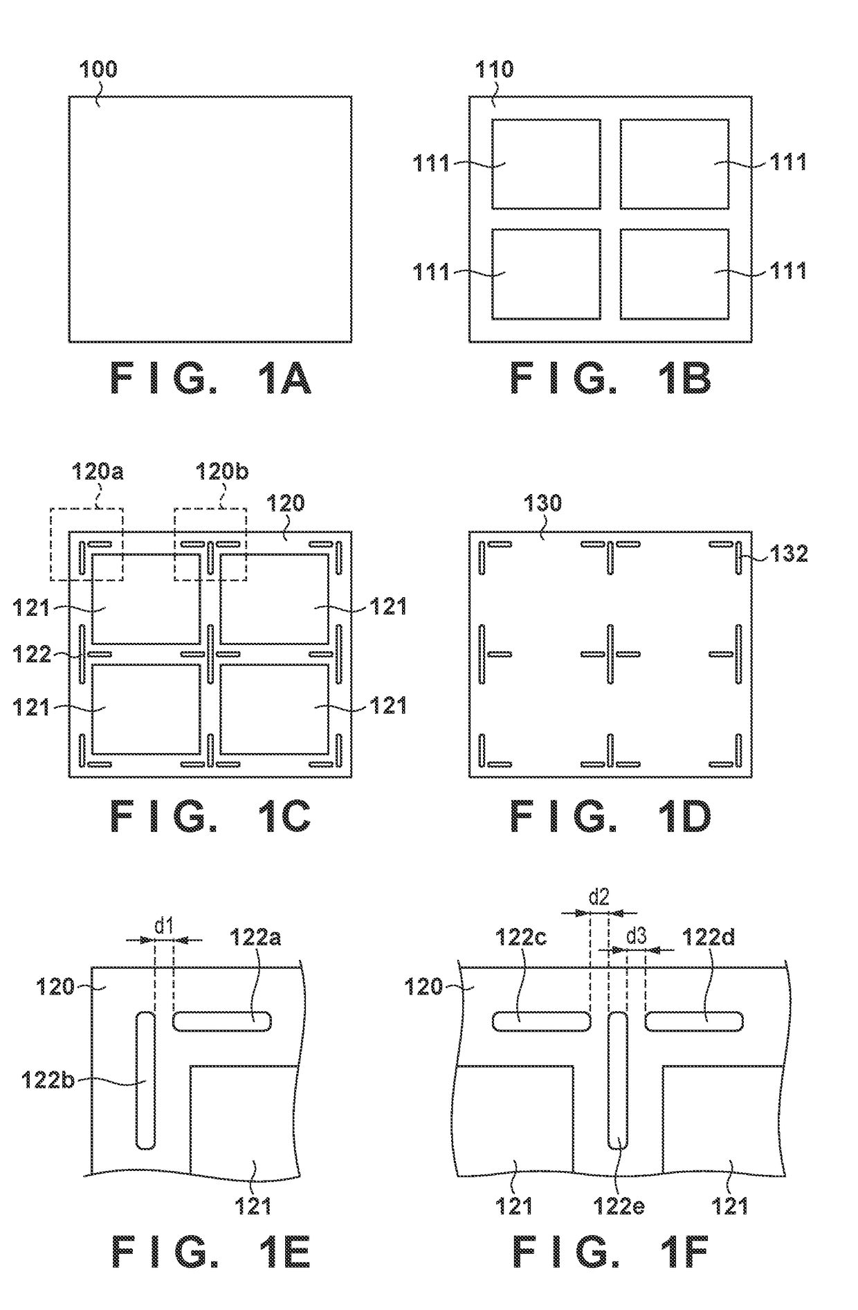
[0019]First, a plurality of ceramic green sheets 100 shown in FIG. 1A are prepared. Each ceramic green sheet 100 is formed by, for example, mixing a power of a ceramic material into a binder and molding this binder into a sheet. Silicon carbide, aluminum nitride, sapphire, alumina, silicon nitride, cermet, yttria, mullite, forsterite, cordierite, zirconia, steatite, or the like may be used as the ceramic material.

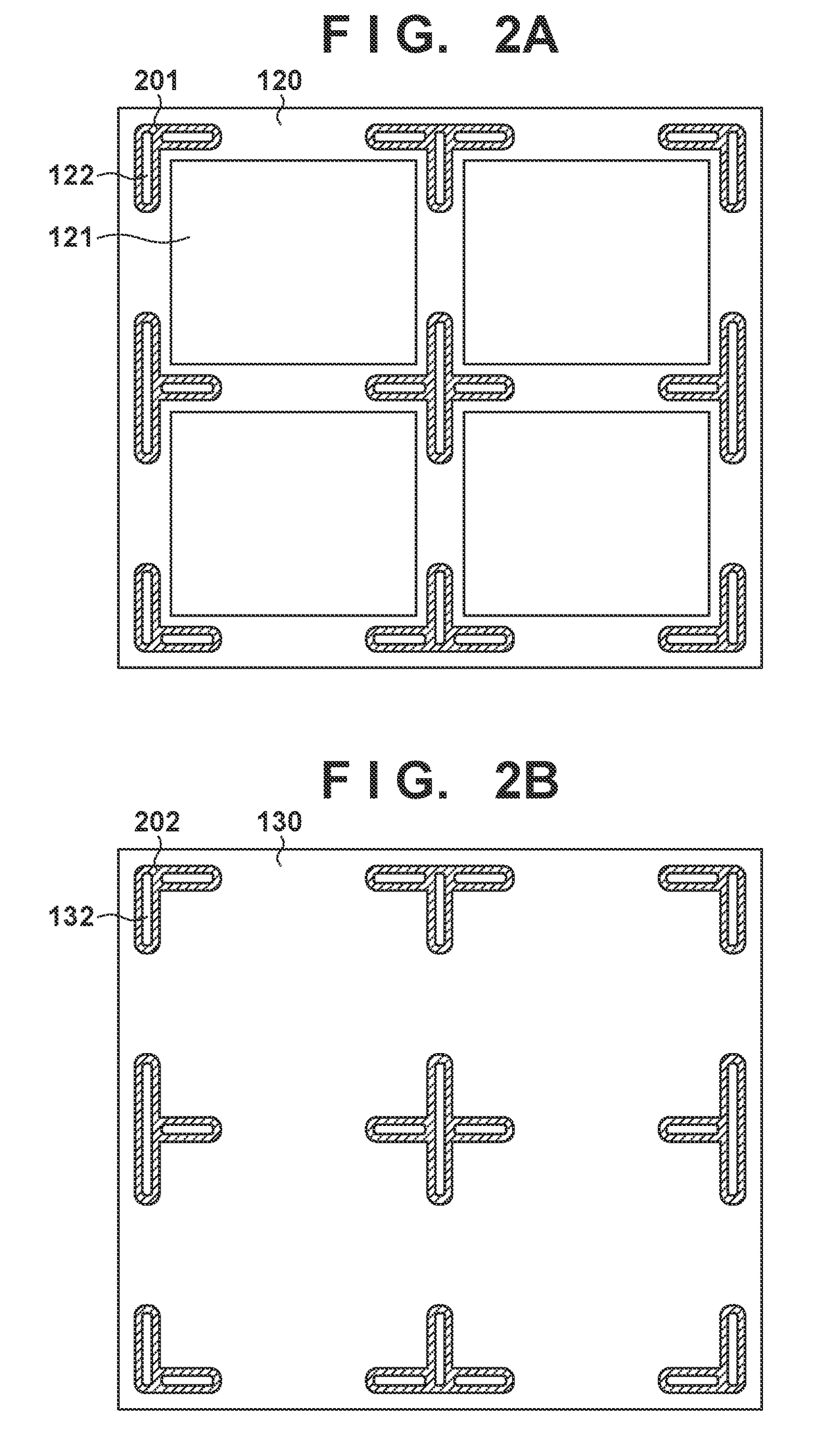
[0020]Then, ceramic green sheets 110, 120, and 130 which are, respectively, shown in FIGS. 1B to 1D are formed as ...

second embodiment

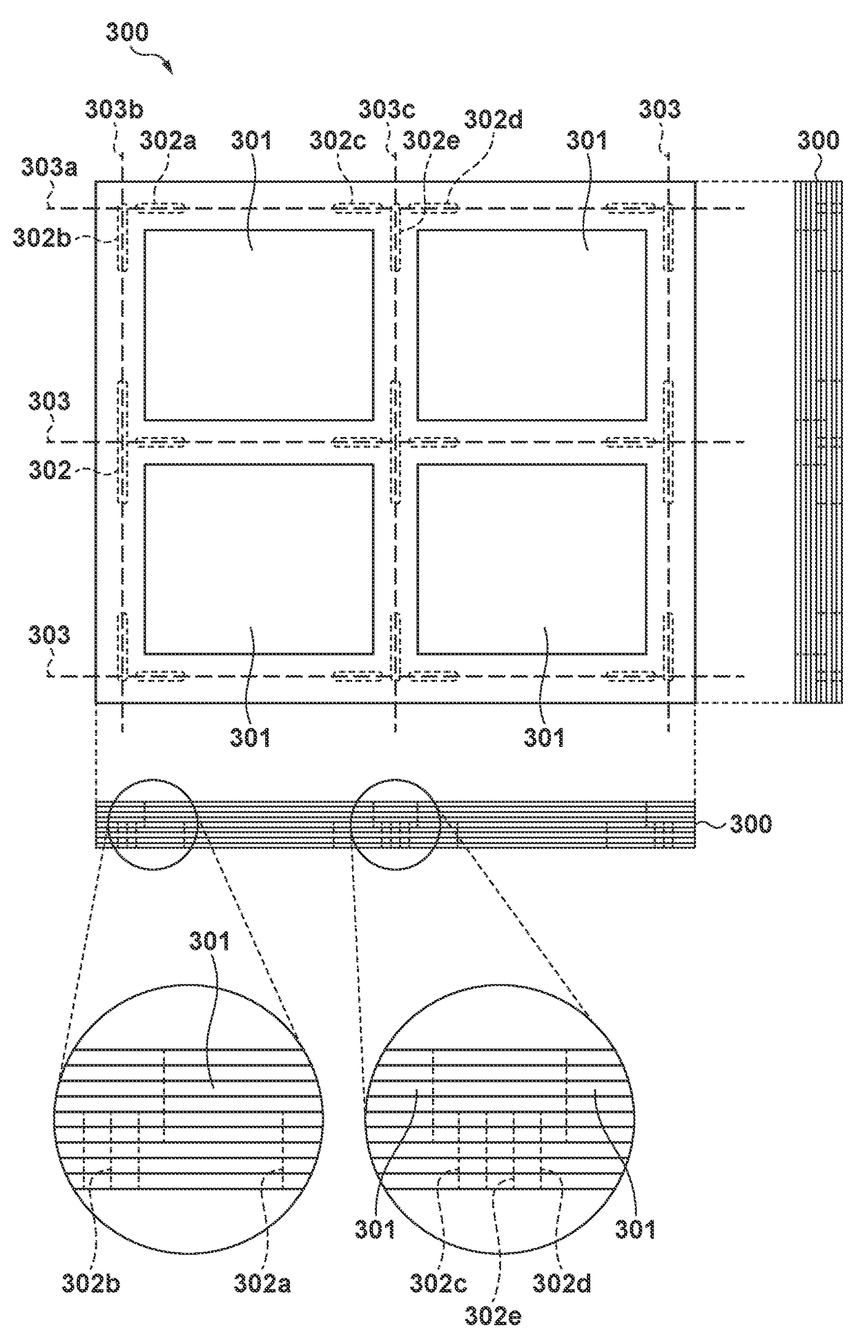
[0055]A method of manufacturing a ceramic package according to the second embodiment will be described with reference to FIGS. 8A to 8D. In the method of manufacturing the ceramic package of the second embodiment, a ceramic green sheet 820 of FIG. 8A is used instead of a ceramic green sheet 120, and a ceramic green sheet 830 of FIG. 8B is used instead of a ceramic green sheet 130. FIG. 8C is an enlarged view showing a portion 820a of the ceramic green sheet 820. FIG. 8D is an enlarged view showing a portion 820b of the ceramic green sheet 820.

[0056]In the second embodiment, the distance between two holes 122 adjacent to each other of the ceramic green sheet 820 is larger than in the first embodiment. As a result, the distance between two connecting portions 402a and 402b adjacent to each other is, for example, larger than each of a height hl of the connecting portion 402a and a height h2 of the connecting portion 402b, and smaller than at least one of a width w1 of the connecting po...

third embodiment

[0059]A method of manufacturing a ceramic package according to the third embodiment will be described with reference to FIGS. 9A to 11. A difference from the first embodiment will mainly be described below. Contents whose description will be omitted in the third embodiment may be the same as in the first embodiment. In the method of manufacturing the ceramic package of the third embodiment, a ceramic green sheet 920 of FIG. 9A is used instead of a ceramic green sheet 120, and a ceramic green sheet 930 of FIG. 9B is used instead of a ceramic green sheet 130. FIG. 9C is an enlarged view showing a portion 920a of the ceramic green sheet 920. FIG. 9D is an enlarged view showing a portion 920b of the ceramic green sheet 920. The ceramic green sheet 920 is different from the ceramic green sheet 120 in that it uses holes 922 instead of holes 122. The ceramic green sheet 930 is different from the ceramic green sheet 130 in that it uses holes 932 instead of holes 132.

[0060]Like the holes 122...


PUM

PropertyMeasurementUnit
diameteraaaaaaaaaa
thicknessaaaaaaaaaa
sizeaaaaaaaaaa

Abstract

A method of manufacturing a ceramic package is provided. An electrically conductive paste is applied to an inside of the first hole and an inside of the second hole of a ceramic green sheet. A ceramic member including first and second electrically conductive members is formed by burning the ceramic green sheet. The ceramic member is divided so as to divide each of the first and second electrically conductive members. A distance between first and second connecting portions is smaller than each of a length of the first connecting portion in a first direction and a length of the second connecting portion in a second direction. The length of the first connecting portion in the first direction is larger than a length of the first connecting portion in a third direction. The length of the second connecting portion has a similar relation.

Description

BACKGROUND OF THE INVENTIONField of the Invention[0001]The present invention relates to a ceramic package, a method of manufacturing the same, an electronic component, and a module.Description of the Related Art[0002]A package for mounting an electronic device has been manufactured by using a ceramic package. Japanese Patent Laid-Open No. 2015-065207 has described a technique of using electrodes arranged on the side surfaces of a ceramic package as connecting portions to be jointed to a mounting board with solder. It is possible, by thus jointing the connecting portions on the side surfaces of the package with solder, to firmly couple the package and the mounting board to each other.SUMMARY OF THE INVENTION[0003]As a method of forming connecting portions on the side surfaces of a ceramic package, a method of forming a hole in a ceramic green sheet, forming an electrically conductive member passing through this hole, and dividing the ceramic green sheet on a plane passing through the...

Claims


Application Information

Patent Timeline
Patent Type & Authority Applications(United States)
IPC IPC(8): H01L23/15H01L23/498H01L21/48H01L23/14
CPCH01L23/15H01L23/49805H01L23/49827H01L2924/15787H01L21/486H01L23/14H01L21/4807
Inventor SHIMIZU, KOICHI
Owner CANON KK
Why Eureka
Try Eureka