Etch residue reduction by ash methodology

a technology of etch residue and reduction method, which is applied in the direction of semiconductor/solid-state device testing/measurement, electrical equipment, basic electric elements, etc., can solve the problems of exacerbating rc delays and additional challenges of incorporating these materials into workable semiconductor fabrication processes, and achieve the effect of improving cd control

Active Publication Date: 2009-07-02
TEXAS INSTR INC
View PDF26 Cites 190 Cited by
  • Summary
  • Abstract
  • Description
  • Claims
  • Application Information

AI Technical Summary

Problems solved by technology

However, incorporating these materials into workable semiconductor fabrication processes presents additional challenges.
This residual polymer, if left uncleaned, causes a high resistance interface between underlying conductive features and the deposited fill or barrier material, thus exacerbating RC delays.

Method used


Image

  • Etch residue reduction by ash methodology
  • Etch residue reduction by ash methodology
  • Etch residue reduction by ash methodology

Examples


Embodiment Construction

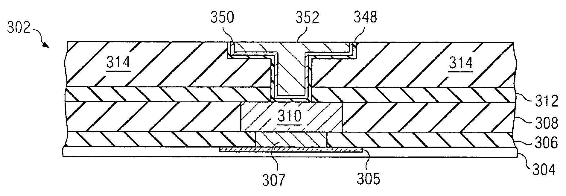
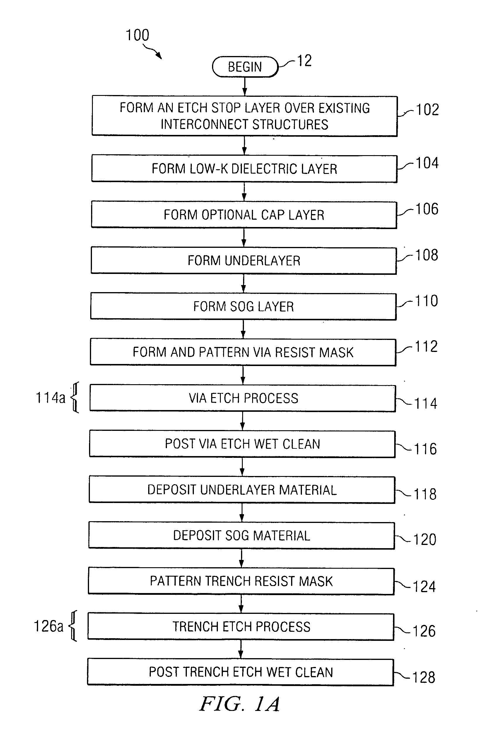
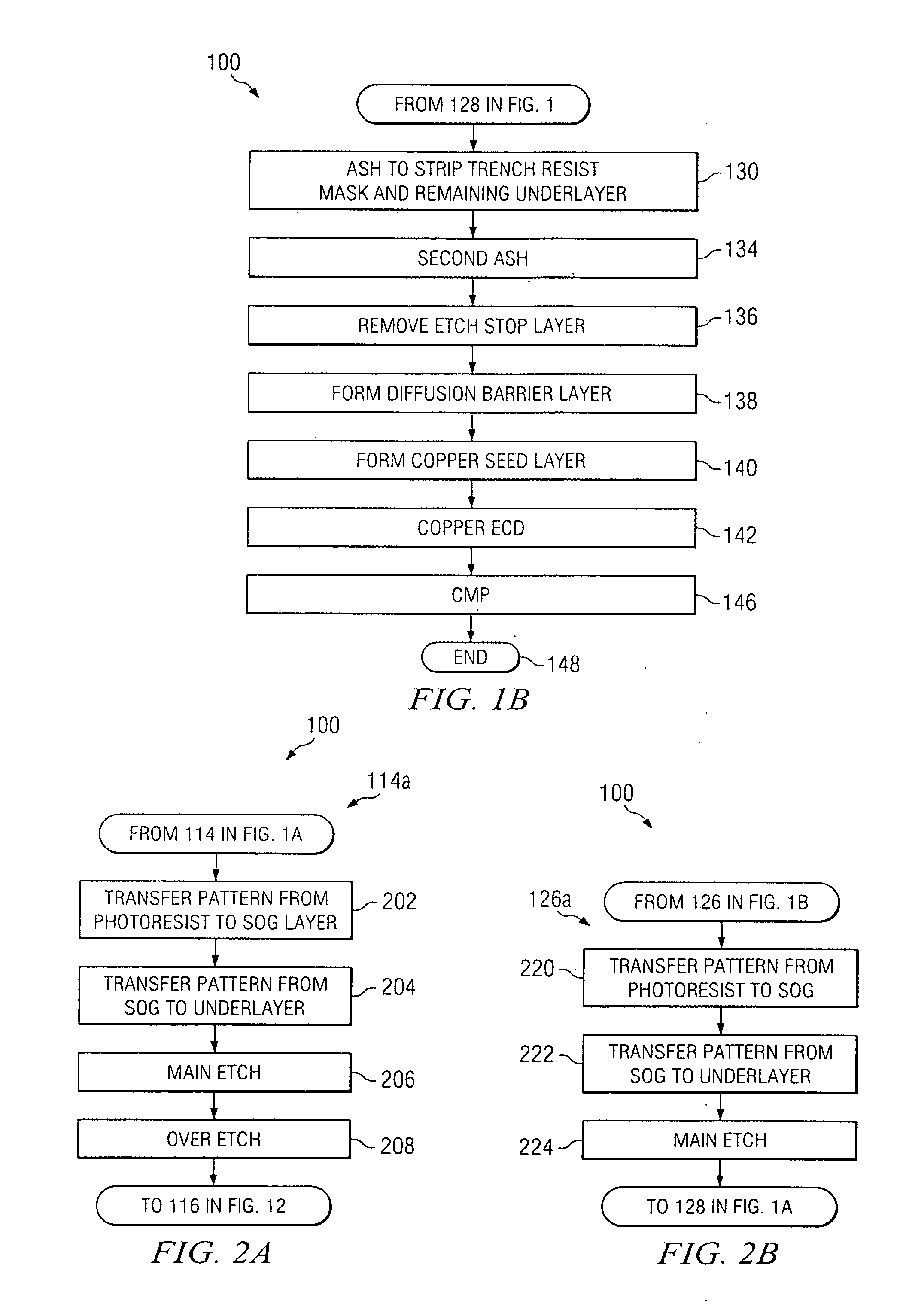
[0017]The present invention will now be described with reference to the attached drawings, wherein like reference numerals are used to refer to like elements throughout. The invention relates to methods for forming single and / or dual damascene interconnect structures, including via and / or trench cavities or openings during interconnect processing of integrated circuits and other semiconductor devices. One or more implementations of the invention are hereinafter illustrated and described in the context of single or dual damascene trench and / or via cavity formation in low-k dielectric structures, wherein silicon nitride (SiN) and / or silicon oxide (SiO) etch-stop layers are employed. However, it will be appreciated by those skilled in the art that the invention is not limited to the exemplary implementations illustrated and described hereinafter. In particular, the various aspects of the invention may be employed in association with processing of devices using OSG, FSG, or other low-k ...


PUM


Abstract

Methods for forming dual damascene interconnect structures are provided. The methods incorporate an ashing operation comprising a first ash operation and a second overash operation. The ashing operation is performed prior to etching of an etch stop layer. The operation removes residue from a cavity formed during formation of the interconnect structure and facilitates better CD control without altering the cavity profiles.

Description

FIELD OF THE INVENTION[0001]The invention relates to semiconductor devices and, more particularly, to a method of reducing etch residue in a dual damascene structure.BACKGROUND OF THE INVENTION[0002]In the manufacture of semiconductor products such as integrated circuits, individual electrical devices are formed on or in a semiconductor substrate, and are thereafter interconnected to form electrical circuits. Interconnection of these devices within an integrated circuit is typically accomplished by forming a multi-level interconnect network in layers formed over the electrical devices, by which the device active elements are connected to one another to create the desired circuits. Individual wiring layers within the multi-level network are formed by depositing an insulating or dielectric layer over the discrete devices or over a previous interconnect layer, and patterning and etching cavities such as vias and trenches. Conductive material, such as copper is then deposited into the c...

Claims


Application Information

Patent Timeline
Patent Type & Authority Applications(United States)
IPC IPC(8): H01L21/66
CPCH01L21/02063H01L21/76814H01L21/76808
Inventor JACQUES, JEANNETTE MICHELLERAMAPPA, DEEPAK A.
Owner TEXAS INSTR INC
Why Eureka
Try Eureka