Low-Loss Optical Interconnect

Active Publication Date: 2009-08-06
CISCO TECH INC
View PDF3 Cites 8 Cited by
  • Summary
  • Abstract
  • Description
  • Claims
  • Application Information

AI Technical Summary

Benefits of technology

[0009]A low-loss optical interconnect, substantially as shown in and/or described in c

Problems solved by technology

However, narrow waveguides have typically high propagation losses due to the interaction of the optical mode with the waveguide surface.
However, these waveguides cannot interface easily to other optical components, nor can they be bent with low optical loss due to mode conversion in the bent sections.
Furthermore, typical narrow waveguide bend designs have intrinsic mismatch losses due to the offset and asymmetry of the optical mode inside a bend.
Such mismatch losses can be mitigated by physically offsetting the two waveguides in the plane of the bend but cannot be fully eliminated by traditional means in high index contrast systems.

Method used


Image

  • Low-Loss Optical Interconnect
  • Low-Loss Optical Interconnect
  • Low-Loss Optical Interconnect

Examples


Embodiment Construction

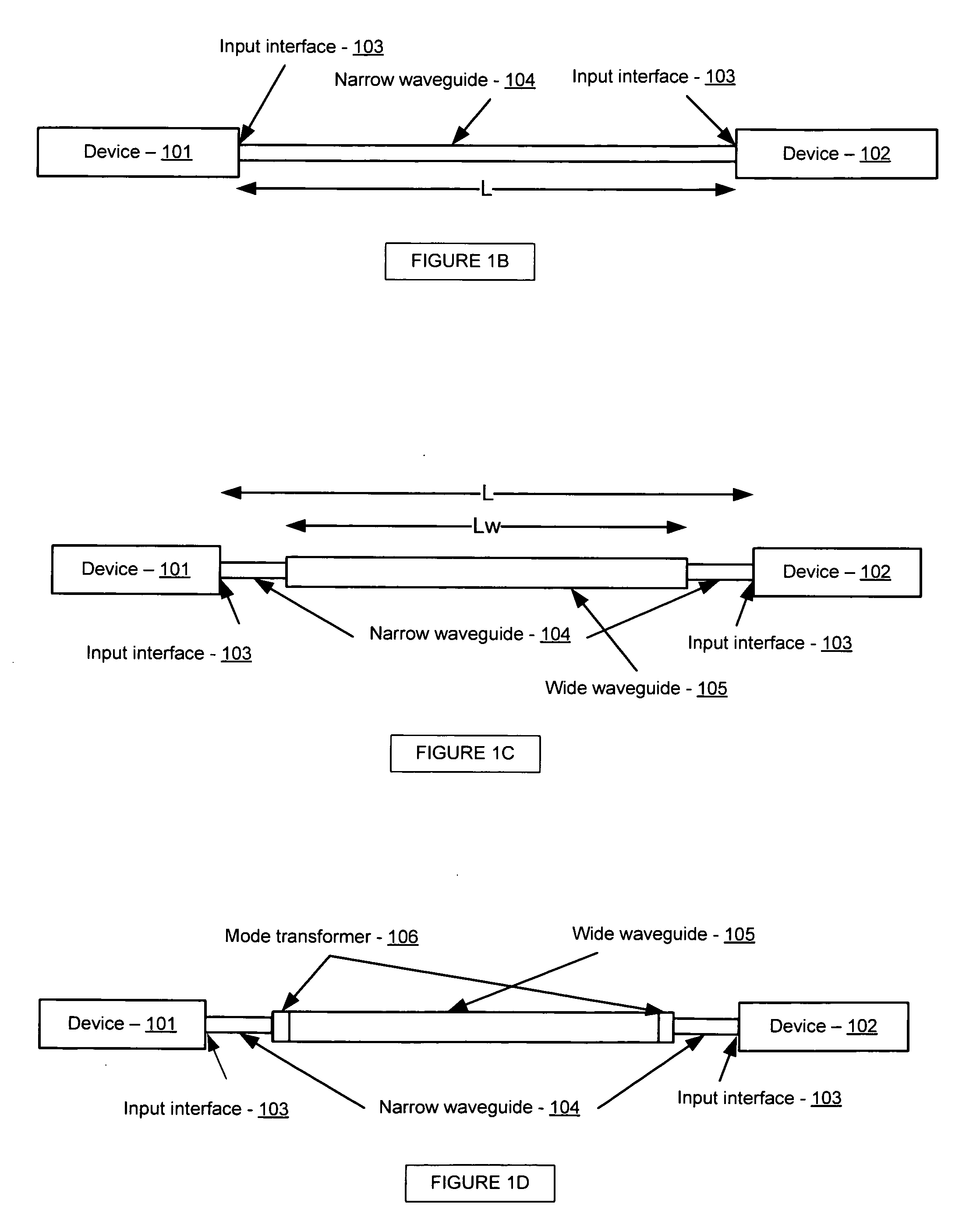
[0022]Certain aspects of the invention may be found in a low-loss optical interconnect. Exemplary aspects of the invention may comprise an optical interconnect system with narrow and wide waveguides joining optical devices. The system may also comprise mode converters and waveguide bends. The waveguides may comprise silicon. Other exemplary aspects of the invention may comprise a continuous optical bend, whose radius of curvature at its endpoints is infinity and at its internal points is finite. The bend may be made of silicon. The width of the bend may vary along the bend. The system may comprise narrow and wide waveguides and a continuous bend.

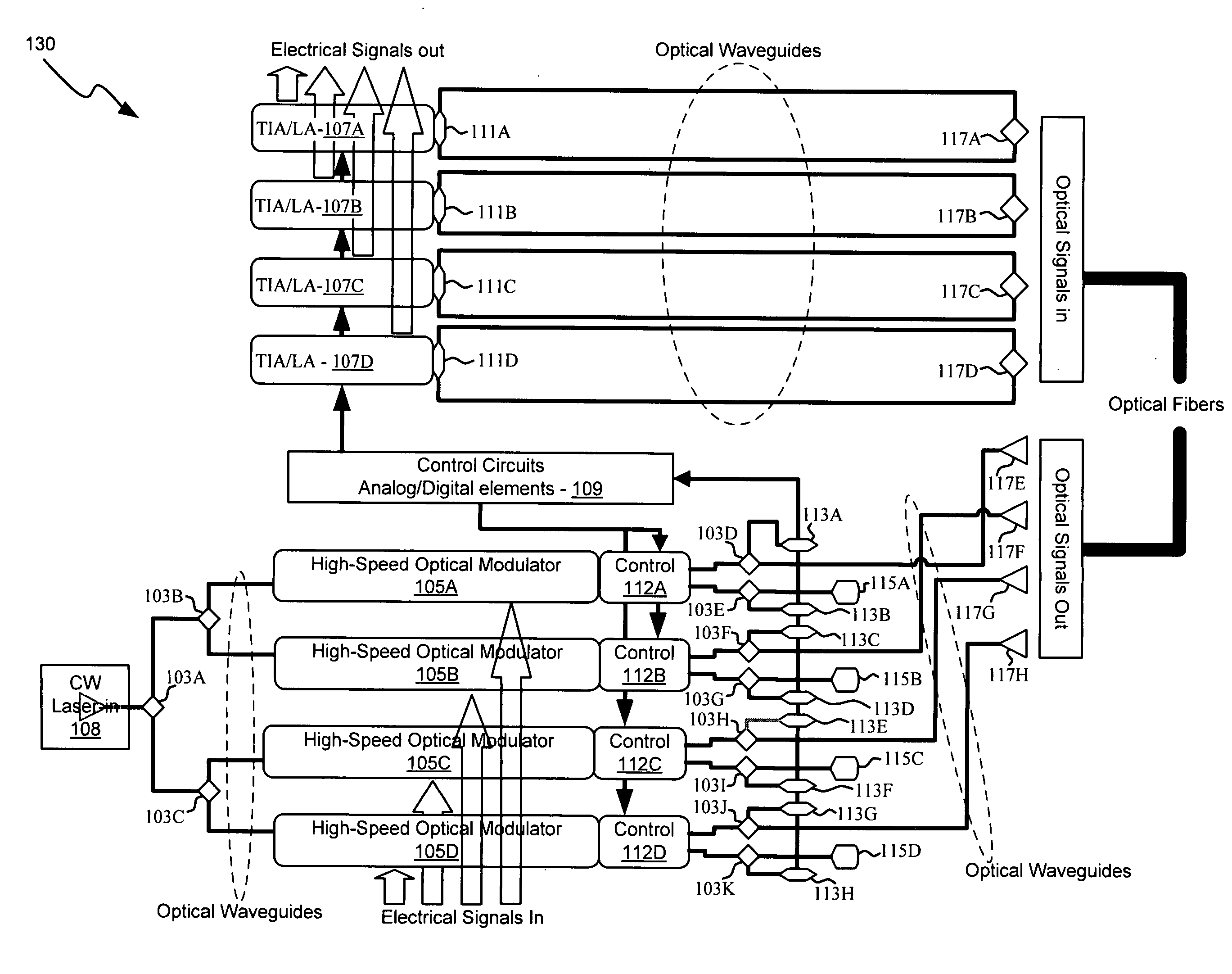
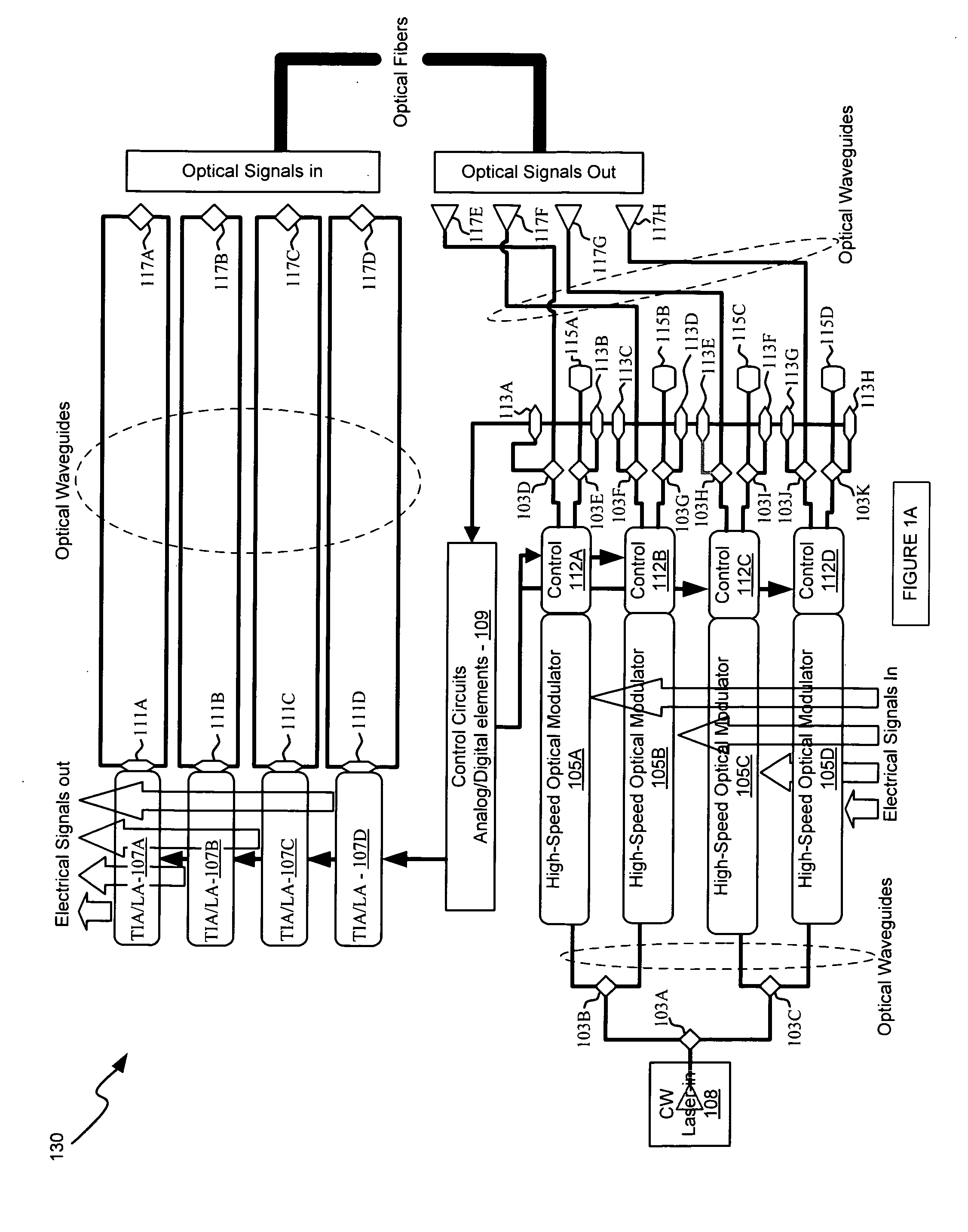
[0023]FIG. 1A is a block diagram of a photonically enabled CMOS chip, in accordance with an embodiment of the invention. Referring to FIG. 1A, there is shown optoelectronic devices on a CMOS chip 130 comprising high speed optical modulators 105A-105D, high-speed photodiodes 111A-111D, monitor photodiodes 113A-113H, and optical devices compri...


PUM


Abstract

A low-loss optical interconnect is disclosed and may include an optical interconnect system with narrow and wide waveguides joining optical devices. The system may also comprise mode converters and waveguide bends. The waveguides may be made of silicon. Other exemplary aspects of the invention may comprise a continuous optical bend, whose radius of curvature at its endpoints is infinity and at its internal points is finite. The bend may be made of silicon. The width of the bend may vary along the bend. The system may comprise narrow and wide waveguides and a continuous bend.

Description

CROSS-REFERENCE TO RELATED APPLICATIONS / INCORPORATION BY REFERENCE[0001]This application makes reference to and claims priority to U.S. Provisional Application Ser. No. 61 / 062,978 filed on Jan. 30, 2008, which is hereby incorporated herein by reference in its entirety.FEDERALLY SPONSORED RESEARCH OR DEVELOPMENT[0002][Not Applicable][MICROFICHE / COPYRIGHT REFERENCE][0003][Not Applicable]FIELD OF THE INVENTION[0004]Certain embodiments of the invention relate to photonic integrated circuits. More specifically, certain embodiments of the invention relate to a low-loss optical interconnect in such circuits.BACKGROUND OF THE INVENTION[0005]Photonic integrated circuits (PICs) integrate many optical functions on a single chip. These circuits require a means of connecting the individual light processing elements inside the circuits to each other. Waveguides, whose operation is based on refractive index contrast, are typical elements that transfer light from one element to the other in optical...

Claims


Application Information

Patent Timeline
IPC IPC(8): G02B6/12
CPCG02B6/14G02B6/12004
Inventor MEKIS, ATTILA
Owner CISCO TECH INC
Why Eureka
Try Eureka