

Oxide semiconductor transistor and method of manufacturing the same
a semiconductor transistor and oxide technology, applied in the direction of transistors, semiconductor devices, electrical devices, etc., can solve the problems of a-si tfts in cost, limited a-si tfts technology, and increased manufacturing costs
- Summary
- Abstract
- Description
- Claims
- Application Information
AI Technical Summary
Benefits of technology
Problems solved by technology
Method used
Image

Examples
Embodiment Construction
[0032]One or more embodiments provide a thin film transistor (TFT) including an oxide semiconductor channel layer. Such an oxide semiconductor TFT according to the embodiments of the present invention can be applied to a driving circuit unit and a pixel unit of a display device such as a liquid crystal display (LCD), an organic light emitting device (OLED), or the like. The oxide semiconductor TFT can instead be applied to just one of the driving circuit unit and the pixel unit.
[0033]Hereinafter, the embodiments will be described in detail with reference to the attached drawings. Like reference numerals in the drawings denote like elements. In the drawings, the sizes or thicknesses of elements are exaggerated for clarity.
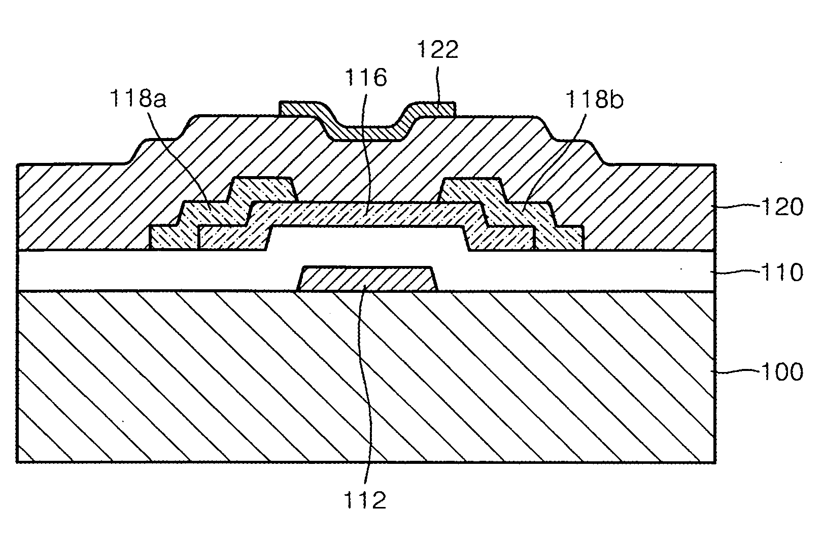
[0034]Turning now to FIG. 1, FIG. 1 is a cross-sectional view of an oxide semiconductor TFT according to an embodiment of the present invention. Referring to FIG. 1, the oxide semiconductor TFT of the present embodiment includes a channel layer 116, a first gate ins...
PUM
 Abstract
Description
Claims
Application Information