Display Panel

a display panel and display pattern technology, applied in the field of display panels, can solve the problems of reducing the detection capability of the touch panel, reducing the detection capability of the above-described detection signal, and significantly increasing the capacitance of the electrode, so as to reduce the viewing pattern of the electrode and improve the accuracy of coordinate detection

Active Publication Date: 2009-08-27
JAPAN DISPLAY INC +1
View PDF10 Cites 276 Cited by
  • Summary
  • Abstract
  • Description
  • Claims
  • Application Information

AI Technical Summary

Benefits of technology

[0016]An advantage of the present invention is that a display panel is provided having a touch panel in which the viewing of the pattern of the electrodes can be reduced and the coordinate detection precision is improved.
[0017]According to various aspects of the present invention, there are provided:
[0018](1) a display panel having, for example, a capacitive touch panel over a display region, wherein the capacitive touch panel comprises a plurality of X electrodes and a plurality of Y electrodes formed with an insulating layer therebetween and in a manner to cross each other, each of the X electrodes and the Y electrodes is formed such that a pad portion and a narrow line portion are alternately placed in a direction of extension, and, when viewed from top, the pad portion of the X electrode and the pad portion of the Y electrode are placed to not overlap each other and a dummy electrode which is in a floating relationship with the X electrode and the Y electrode is formed between the pad portion of the X electrode and the pad portion of the Y electrode;
[0019](2) the display panel according to, for example, (1), wherein the dummy electrode between the pad portion of the X electrode and the pad portion of the Y electrode comprises a plurality of electrodes which are aligned from the pad portion of the X electrode to the pad portion of the Y electrode;
[0020](3) the display panel according to, for example, (1) or (2), wherein the dummy electrode is formed in a same layer as the X electrode;
[0021](4) the display panel according to, for example, (1) or (2), wherein the dummy electrode is formed in a same layer as the Y electrode;

Problems solved by technology

In this case, if the space α is widened, there is a disadvantage that, because of a difference in transmittance of light between the portion of the space and the portion where the electrode is formed or because of a difference in a reflective characteristic caused by a difference in the vertical structure as shown in FIG. 16, the pattern of the X electrode XP or the pattern of the Y electrode YP is viewed.
If, on the other hand, the space α is narrowed, and an overlap occurs between the X electrode XP and the Y electrode YP due to a deviation of a mask during manufacturing, the electrode capacitance (Cx or Cy) is significantly increased, and there is a disadvantage that the above-described detection signal proportional to Cf / {Cx×(Cf+CX)} becomes small.
In addition, even when there is no overlap between the X electrode XP and the Y electrode YP, when the space α is significantly reduced, a fringe capacitance between the electrodes is increased, resulting in the disadvantage as described above, and degradation in the detection capability of the touch panel.

Method used


Image

  • Display Panel
  • Display Panel
  • Display Panel

Examples


first preferred embodiment

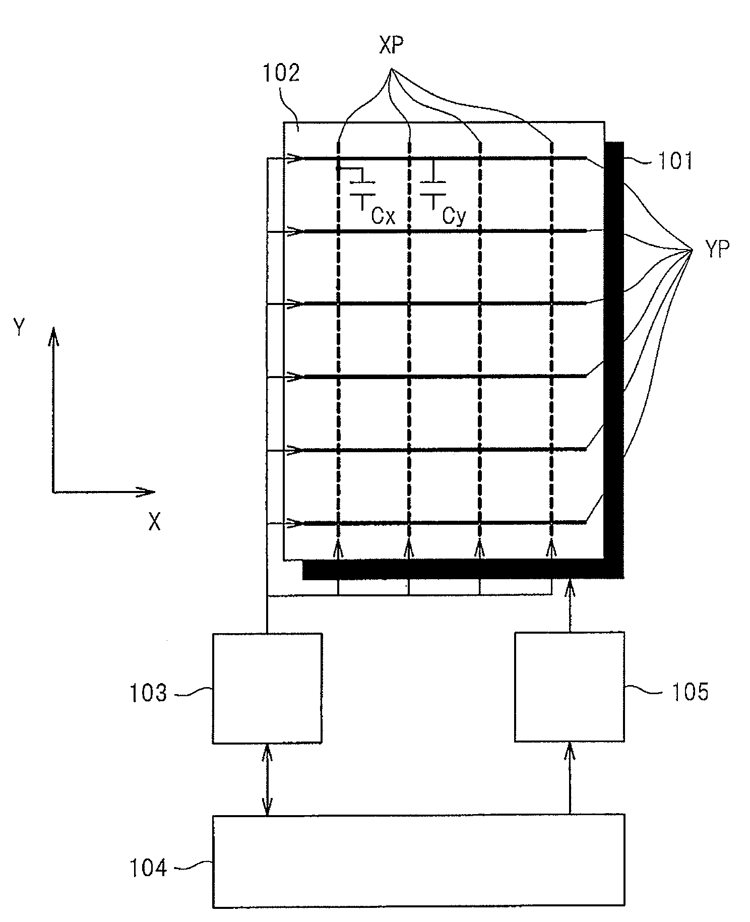
[0054]FIG. 1 is a structural diagram showing a preferred embodiment of a display panel of the present invention, along with a touch panel and a driving circuit of the touch panel. A touch panel 102 is placed over a display region of a display panel (display) 101. The touch panel 102 comprises an X electrode XP and a Y electrode YP with an insulating film (not shown) therebetween. The X electrode XP comprises a plurality of electrodes which extend along a y direction in FIG. 1 and which are aligned along an x direction, and detects a coordinate in the x direction. The Y electrode YP comprises a plurality of electrodes which extend along the x direction and which are aligned along the y direction, and detects a coordinate in the y direction. The touch panel 102 is formed with a transparent member including the X electrode XP and the Y electrode YP so that the display panel 101 can be viewed through the touch panel 102. The X electrode XP and the Y electrode YP are connected to a detec...

second preferred embodiment

[0073]FIG. 7 is a plan view showing another preferred embodiment of the touch panel 102, and which corresponds to FIG. 3. FIG. 8 is a cross sectional view along an VIII-VIII line of FIG. 7.

[0074]A structure in FIG. 7 which differs from FIG. 3 is that, for the dummy electrode XD formed adjacent to each side of the pad portion of the X electrode XP, two aligned dummy electrodes CS are formed in a direction crossing each side of the pad portion. In addition, for the Y electrode YP also, the dummy electrode YD is provided adjacent to each side of the pad portion, and, for the dummy electrode YD, two aligned dummy electrodes YD are provided in a direction crossing each side of the pad portion. With such a configuration also, advantages similar to those in the first preferred embodiment can be obtained.

[0075]Alternatively, the number of dummy electrodes may be three or more. The plurality of dummy electrodes can similarly be formed in a same layer as one electrode of the X electrode XP an...

third preferred embodiment

[0076]FIG. 9 is a plan view showing another preferred embodiment of the touch panel 102, and which corresponds to FIG. 3. FIG. 10 is a cross sectional view along a X-X line of FIG. 9.

[0077]A structure different from FIG. 3 is that a dummy electrode XD (shown with reference sign XDc in FIG. 9) in a floating state and electrically insulated from the X electrode XP is formed at a center of a pad portion of the X electrode XP and a dummy electrode YD (shown in FIG. 9 with reference sign YDc) in a floating state and electrically insulated from the Y electrode YP is formed at a center of the pad portion of the Y electrode YP.

[0078]With such a configuration, for example, at the X electrode XP, the capacitance Cxs between the shield layer SLD and the X electrode XP can be reduced. Therefore, the electrode capacitance Cx can be reduced and the signal component can be improved. In addition, when a conductor such as a finger reaches the dummy electrode XDc at the center of the pad portion of t...


PUM


Abstract

A display panel is provided having a capacitive touch panel over a display region, wherein the capacitive touch panel comprises a plurality of X electrodes and a plurality of Y electrodes formed with an insulating layer there between and in a manner to cross each other, each of the X electrodes and the Y electrodes is formed such that a pad portion and a narrow line portion are alternately placed in a direction of extension, and when viewed from top, the pad portion of the X electrode and the pad portion of the Y electrode are placed to not overlap each other and a dummy electrode which is in a floating relationship with the X electrode and the Y electrode is formed between the pad portion of the X electrode and the pad portion of the Y electrode.

Description

CROSS-REFERENCE TO RELATED APPLICATIONS[0001]The present application claims priority from Japanese application JP 2008-045538 filed on Feb. 27, 2008, the content of which is hereby incorporated by reference into this application.BACKGROUND OF THE INVENTION[0002]1. Field of the Invention[0003]The present invention relates to a display panel.[0004]2. Description of the Related Art[0005]In a display panel having a capacitive touch panel over a display region, the display region can be viewed through the capacitive touch panel (hereinafter simply referred to as “touch panel”), and a predetermined location on the display region can be designated through, for example, contact of a finger or the like on the touch panel.[0006]In the touch panel, a plurality of X electrodes and a plurality of Y electrodes are formed with an insulating film therebetween in a shape crossing each other, and a change of a capacitance due to contact of a finger can be detected. That is, the touch panel is configu...

Claims


Application Information

Patent Timeline
Patent Type & Authority Applications(United States)
IPC IPC(8): G06F3/044
CPCG06F3/044G06F3/0446G06F3/0445G06F3/0412G06F2203/04111G06F3/0448G02F1/13338
Inventor MAMBA, NORIOFURUHASHI, TSUTOMUSATO, HIDEO
Owner JAPAN DISPLAY INC
Why Eureka
Try Eureka