Light emitting diode and method
- Summary
- Abstract
- Description
- Claims
- Application Information
AI Technical Summary
Benefits of technology
Problems solved by technology
Method used
Image

Examples
Embodiment Construction
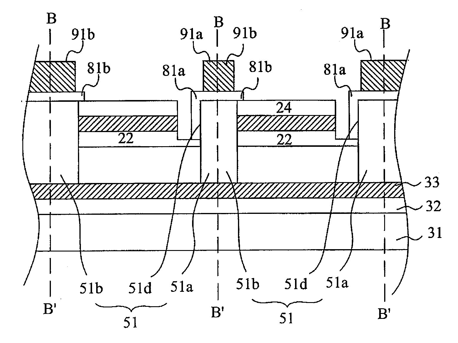
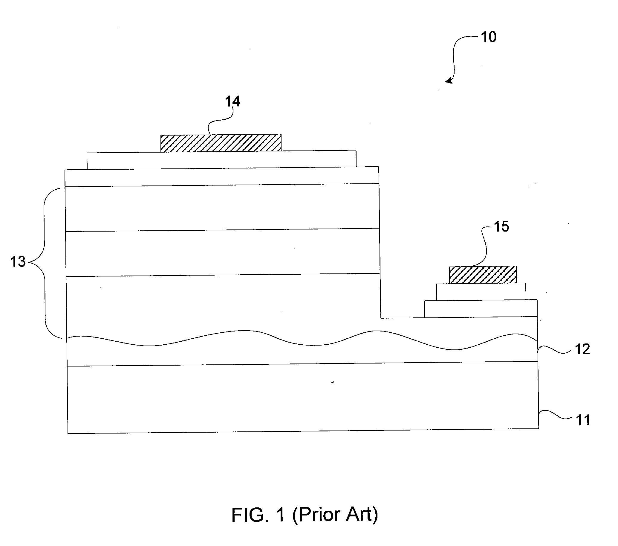
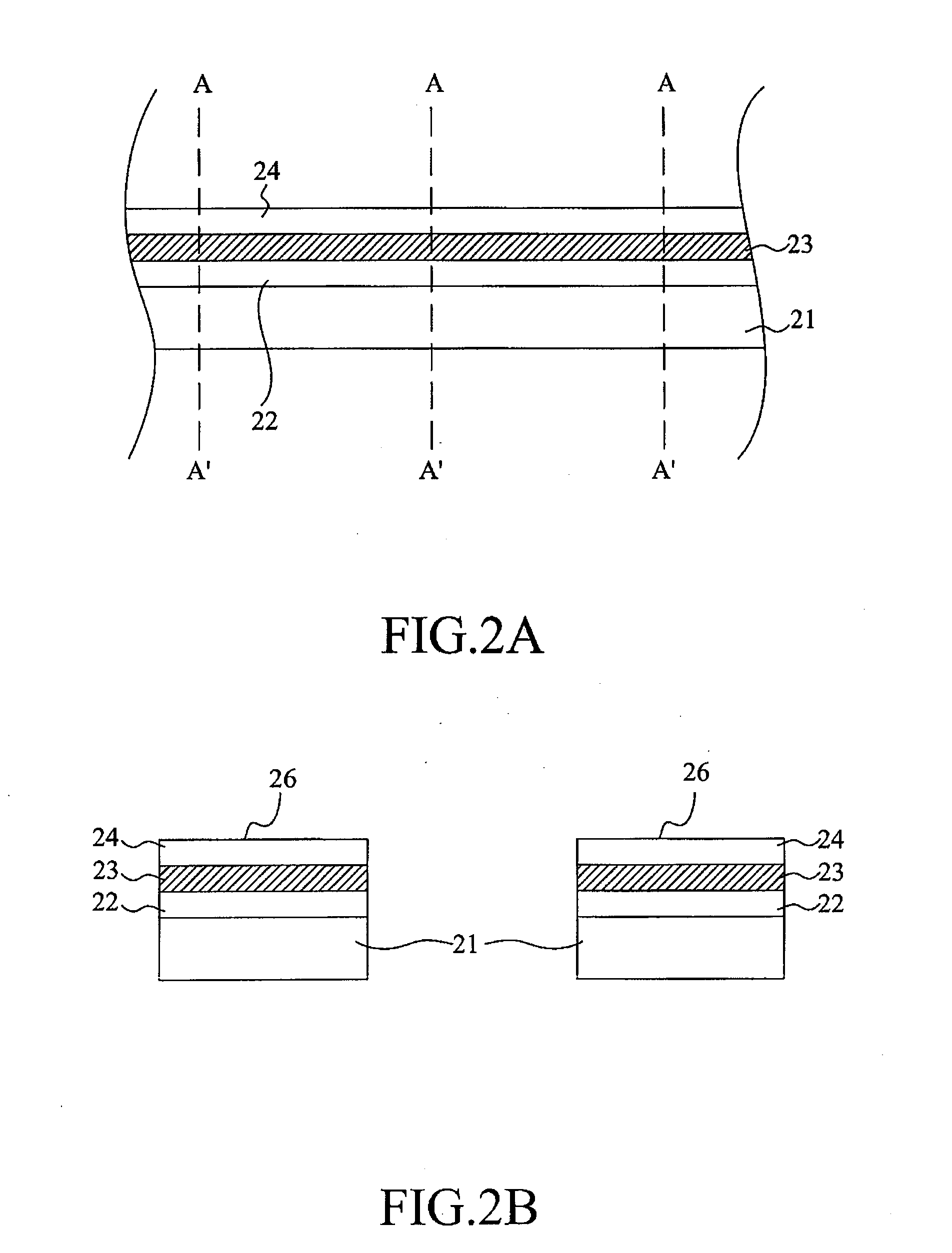
[0012]The preferred embodiments of the present invention will now be described in greater details by referring to the drawings that accompany the present application. It should be noted that the features illustrated in the drawings are not necessarily drawn to scale. Descriptions of well-known components, materials, and process techniques are omitted so as to not unnecessarily obscure the embodiments of the invention. Any devices, components, materials, and steps described in the embodiments are only for illustration and not intended to limit the scope of the present invention.
[0013]In one embodiment of the present invention, a method of forming a light emitting diode is disclosed. As shown in FIG. 2A to FIG. 2B, the method comprises providing an epitaxial structure that includes a first conductive semiconductor layer and a second conductive semiconductor layer. As shown in FIG. 2A, a substrate 21 such as n-type GaAs substrate is provided. Thereafter, the process proceeds to form an...
PUM
 Abstract
Description
Claims
Application Information
 - Generate Ideas
- Intellectual Property
- Life Sciences
- Materials
- Tech Scout
- Unparalleled Data Quality
- Higher Quality Content
- 60% Fewer Hallucinations
Browse by: Latest US Patents, China's latest patents, Technical Efficacy Thesaurus, Application Domain, Technology Topic, Popular Technical Reports.
© 2025 PatSnap. All rights reserved.Legal|Privacy policy|Modern Slavery Act Transparency Statement|Sitemap|About US| Contact US: help@patsnap.com