Non-volatile semiconductor storage device and method of manufacturing the same
Active Publication Date: 2009-09-17
KIOXIA CORP
View PDF1 Cites 117 Cited by
Summary
Abstract
Description
Claims
Application Information
AI Technical Summary
This helps you quickly interpret patents by identifying the three key elements:
Problems solved by technology
Method used
Benefits of technology
Benefits of technology
[0013]Yet another aspect of the present invention provides a method of manufacturing a non-volatile semiconductor storage device having a plurality of memory strings with a plurality of electrically rewritable memory cells connected in series, the method comprising: alternately laminating conductive layers and interlayer insulation layers; forming a hole to penetrate the plurality of conductive layers and interlayer insulation layers; forming a memory gate insulation layer on respective sidewalls, facing the hole, of the conductive layers and interlayer insulation layers; and forming a
Problems solved by technology
Although some measures have been taken to reduce the dimension for each device (refinement) to increase memory storage capacity, recent years are facing challenges in such refinement from the viewpoint of cost and technology.
However, in currently available ArF immersion lithography technology, for example, the resolution limit has been reached around the 40 nm design rule and so EUV exposure devices have to be introduced for further refinement.
However, the EUV exposure devices are expensive and infeasible in view of the costs.
In addition, if such refinement is accomplished, it is assumed that physical improvement limit, such as in breakdown volt
Method used
Image
Click on the blue label to locate the original text in one second.
Reading with bidirectional positioning of images and text.
Examples
first embodiment
Configuration of Non-Volatile Semiconductor Storage Device 100 in First Embodiment
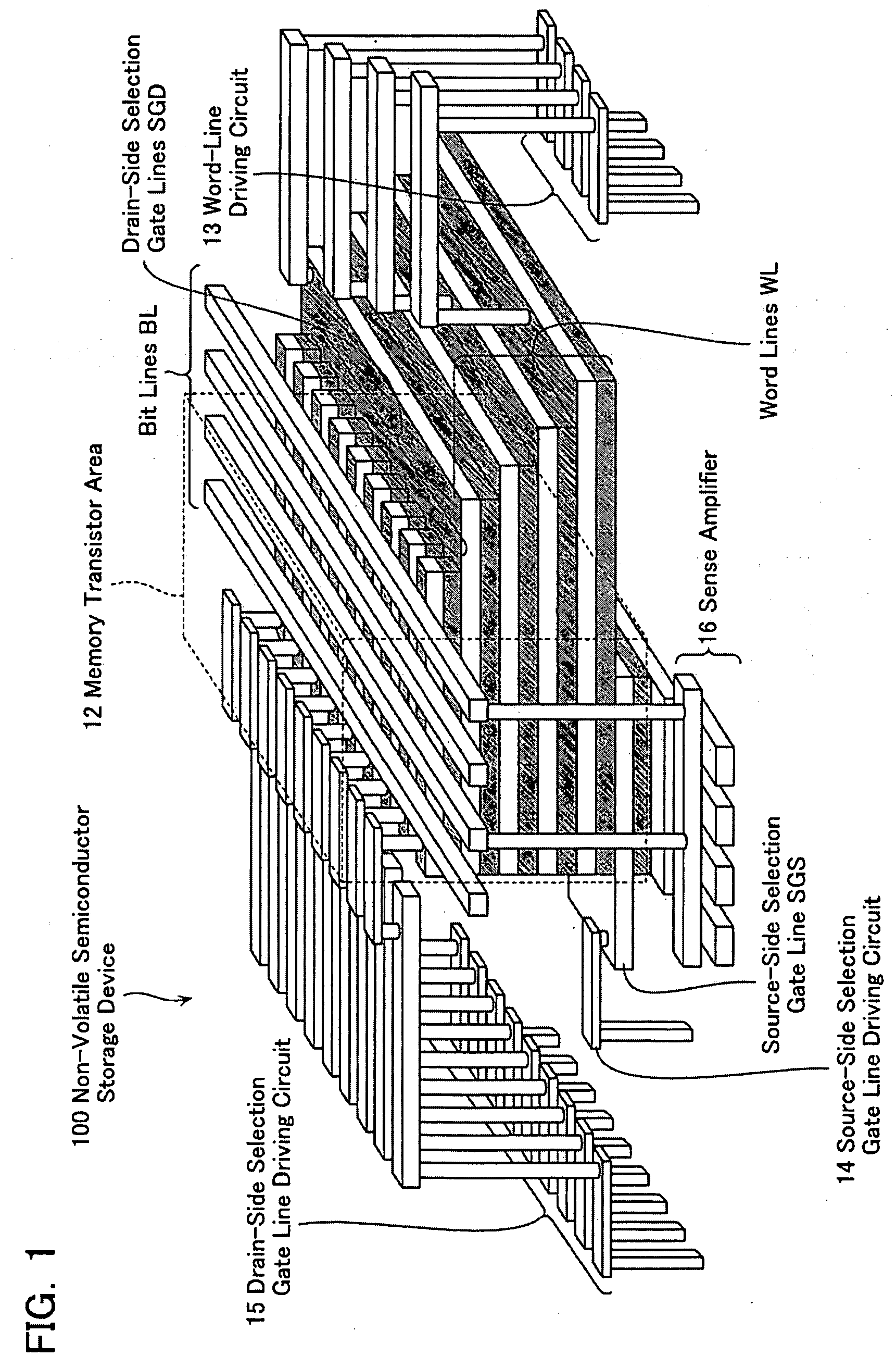
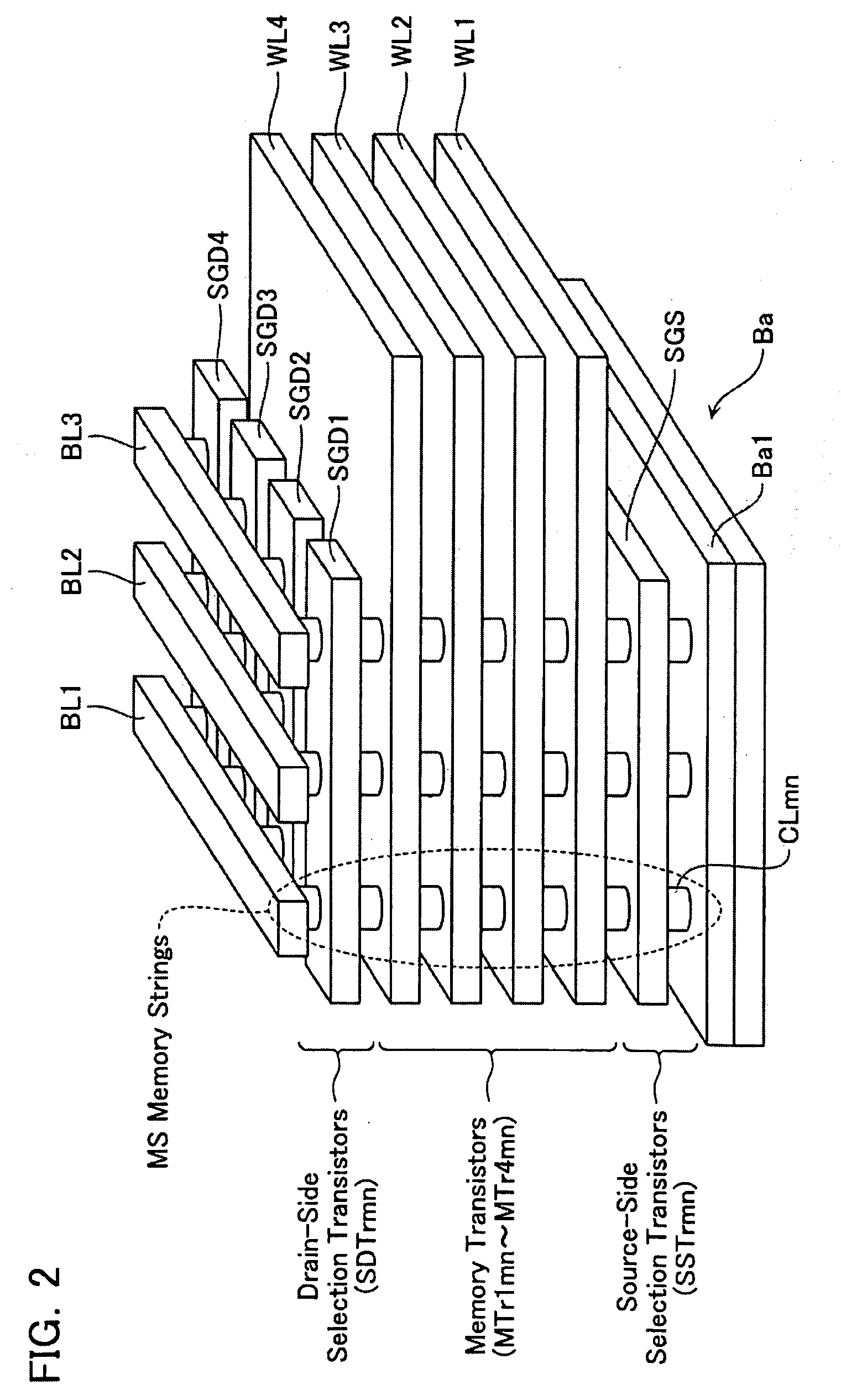
[0036]FIG. 1 schematically illustrates a non-volatile semiconductor storage device 100 according to a first embodiment of the present invention. As illustrated in FIG. 1, the non-volatile semiconductor storage device 100 according to the first embodiment mainly comprises: a memory transistor area 12; a word-line driving circuit 13; a source-side selection gate line (SGS) driving circuit 14; a drain-side selection gate line (SGD) driving circuit 15; and a sense amplifier 16. The memory transistor area 12 has memory transistors for storing data. The word-line driving circuit 13 controls voltage applied to word lines WL. The source-side selection gate line (SGS) driving circuit 14 controls voltage applied to the source-side selection gate line SGS. The drain-side selection gate line (SGD) driving circuit 15 controls voltage applied to drain-side selection gate lines (SGD). The sense amplifier 16 amplifies...
second embodiment
Specific Configuration of Non-Volatile Semiconductor Storage Device in Second Embodiment
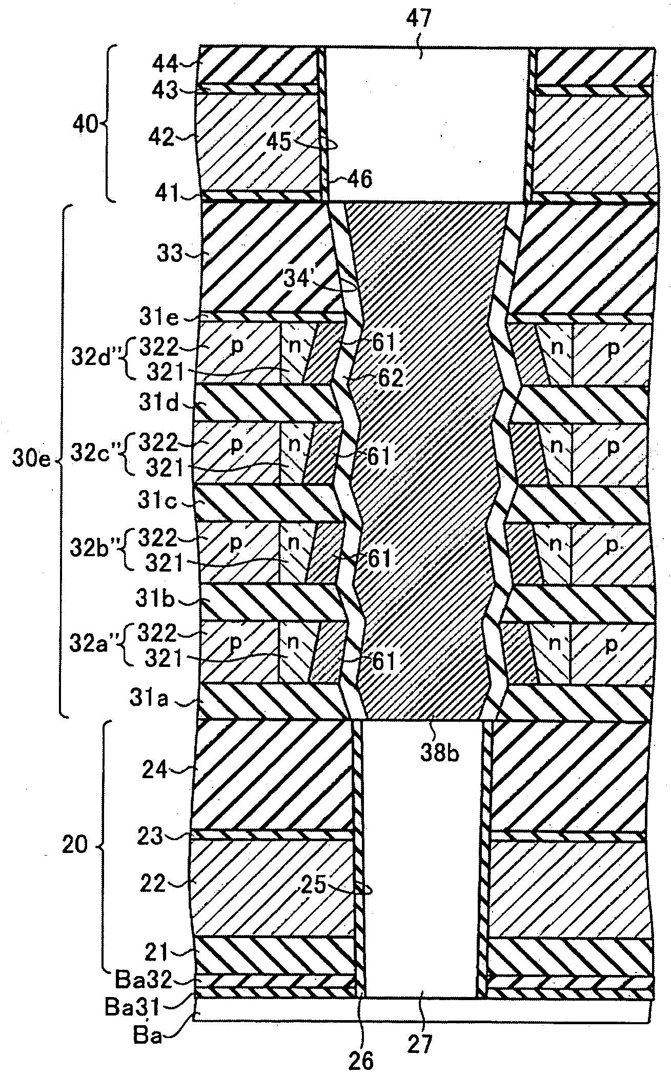
[0084]Referring now to FIG. 11, a specific configuration of a non-volatile semiconductor storage device according to a second embodiment of the present invention will be described below. FIG. 11 is a cross-sectional view of the non-volatile semiconductor storage device configuring one memory string MS according to the second embodiment. Note that the same reference numerals represent the same components as the first embodiment and description thereof will be omitted in the second embodiment.
[0085]As illustrated in FIG. 11, the non-volatile semiconductor storage device (one memory string) of the second embodiment has a memory transistor layer 30a different from the first embodiment.
[0086]The memory transistor layer 30a has first to fourth wordline conductive layers 32a′ to 32d′, a memory hole 34′, a block insulation layer (first insulation layer) 35b, charge accumulation layers 36b, tunnel insulat...
third embodiment
Specific Configuration of Non-Volatile Semiconductor Storage Device in Third Embodiment
[0101]Referring now to FIG. 16, a specific configuration of a non-volatile semiconductor storage device according to a third embodiment of the present invention will be described below. FIG. 16 is a cross-sectional view of the non-volatile semiconductor storage device configuring one memory string MS according to the third embodiment. Note that the same reference numerals represent the same components as the first and second embodiments and description thereof will be omitted in the third embodiment.
[0102]As illustrated in FIG. 16, the non-volatile semiconductor storage device (one memory string) of the third embodiment has a memory transistor layer 30b different from the second embodiment.
[0103]The memory transistor layer 30b has charge accumulation layers 36d different from the second embodiment.
[0104]The charge accumulation layers 36d are formed only on the sidewall of the block insulation lay...
PUM
Abstract
A non-volatile semiconductor storage device has a plurality of memory strings with a plurality of electrically rewritable memory cells connected in series. Each of the memory strings includes: a columnar semiconductor layer extending in a direction perpendicular to a substrate; a plurality of conductive layers formed at a sidewall of the columnar semiconductor layer via memory layers; and interlayer insulation layers formed above of below the conductive layers. A sidewall of the conductive layers facing the columnar semiconductor layer is formed to be inclined such that the distance thereof from a central axis of the columnar semiconductor layer becomes larger at lower position thereof than at upper position thereof. While, a sidewall of the interlayer insulation layers facing the columnar semiconductor layer is formed to be inclined such that the distance thereof from a central axis of the columnar semiconductor layer becomes smaller at lower position thereof than at upper position thereof.
Description
CROSS-REFERENCE TO RELATED APPLICATIONS [0001]This application is based upon and claims the benefit of priority from the prior Japanese Patent Application No. 2008-65886, filed on Mar. 14, 2008, the entire contents of which are incorporated herein by reference.BACKGROUND OF THE INVENTION [0002]1. Field of the Invention[0003]The present invention relates to an electrically rewritable non-volatile semiconductor storage device and a method of manufacturing the same.[0004]2. Description of the Related Art[0005]Conventionally, LSIs are formed by integration of devices in a two-dimensional plane on the silicon substrate. Although some measures have been taken to reduce the dimension for each device (refinement) to increase memory storage capacity, recent years are facing challenges in such refinement from the viewpoint of cost and technology. Such refinement requires further improvements in photolithography technology. However, in currently available ArF immersion lithography technology, ...
Claims
Application Information
Patent Timeline
Application Date:The date an application was filed.
Publication Date:The date a patent or application was officially published.
First Publication Date:The earliest publication date of a patent with the same application number.
Issue Date:Publication date of the patent grant document.
PCT Entry Date:The Entry date of PCT National Phase.
Estimated Expiry Date:The statutory expiry date of a patent right according to the Patent Law, and it is the longest term of protection that the patent right can achieve without the termination of the patent right due to other reasons(Term extension factor has been taken into account ).
Invalid Date:Actual expiry date is based on effective date or publication date of legal transaction data of invalid patent.

