Light emitting device and light emitter

a light emitting device and light emitting element technology, which is applied in the direction of discharge tube luminescnet screens, lighting and heating apparatus, instruments, etc., can solve the problems of uneven emission color, light extraction efficiency deterioration with time, and uneven transparent resin material deterioration by light or heat discharged from the light emitting element, etc., to reduce sense unevenness. , the effect of reducing the difference in chromaticity

Active Publication Date: 2008-11-20
TOYODA GOSEI CO LTD
View PDF6 Cites 69 Cited by
  • Summary
  • Abstract
  • Description
  • Claims
  • Application Information

AI Technical Summary

Benefits of technology

[0044]The above light emitter allows light from the light emitting device to be imaged on the irradiated surface. Where there is provided the irradiated surface, a viewer can sensitively sense unevenness in chromaticity since the difference in chromaticity of light emitted from the light emitting dev...

Problems solved by technology

However, the light emitting devices of JP-A-2004-111882 and JP-A-2005-093896 have a problem that the transparent resin material is likely to deteriorate by light or heat discharged from the light emitting element.
Especially, when using the light emitting element of group III nitride-based compound semiconductor to emit a short wa...

Method used


Image

  • Light emitting device and light emitter
  • Light emitting device and light emitter
  • Light emitting device and light emitter

Examples


first embodiment

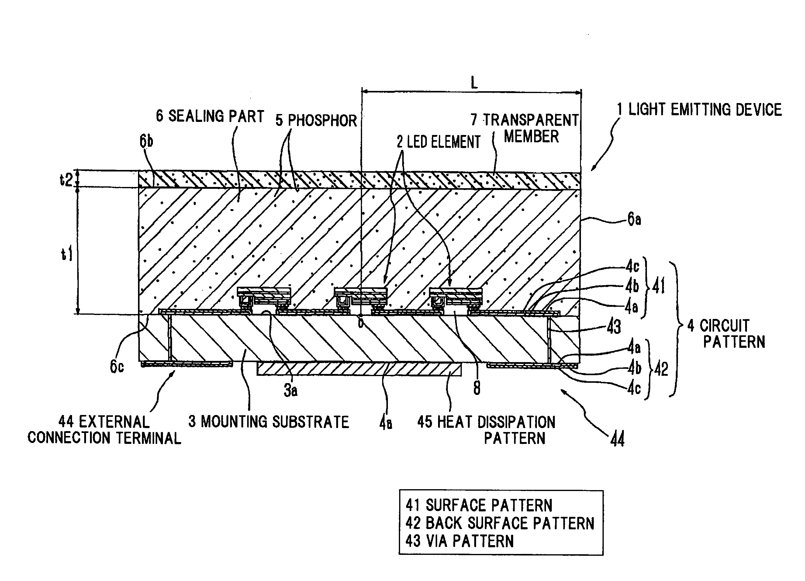
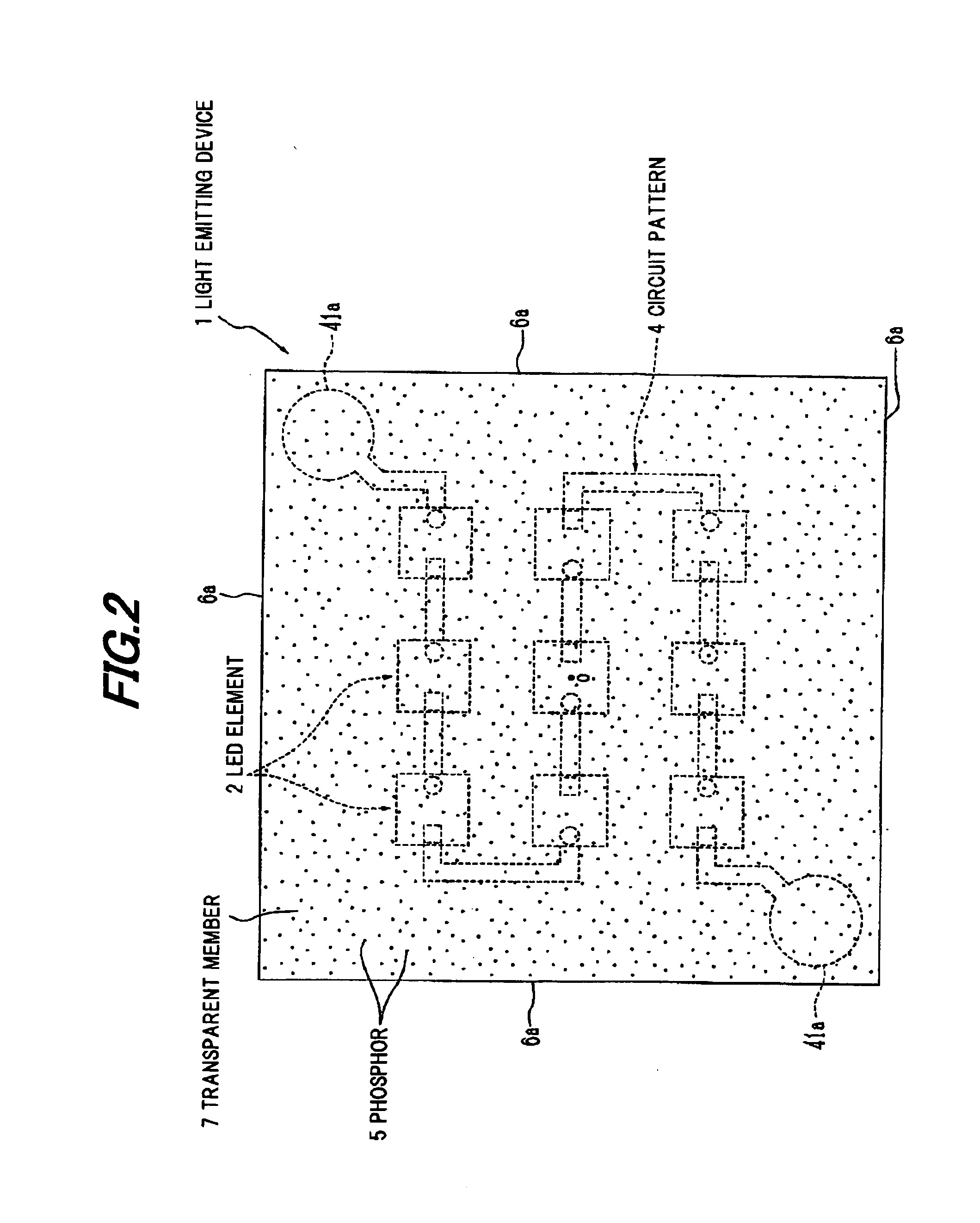
[0066]FIGS. 1 to 3 each shows the first preferred embodiment of the invention, where FIG. 1 is a cross sectional view showing a light emitting device of the first preferred embodiment according to the invention.

[0067]As shown in FIG. 1, the light emitting device 1 comprises plural flip-chip type LED elements 2 formed of GaN-based semiconductor material, a mounting substrate 3 with a mounting surface 3a on which the LED elements 2 are mounted, a circuit pattern 4 formed on the mounting substrate 3 and formed of tungsten (W)-nickel (Ni)-gold (Au), a sealing part 6 for sealing the LED elements 2 on the mounting surface 3a of the mounting substrate 3 and formed of glass with phosphor 5 dispersed therein, and a transparent member 7 formed on the sealing part 6 and having the phosphor 5 dispersed therein. Between the LED elements 2 and the mounting substrate 3, a space 8 is formed into which no glass penetrates.

[0068]The LED elements 2 as a light emitting element are fabricated by epitaxi...

second embodiment

[0098]FIGS. 4 and 5 illustrate a second preferred embodiment according to the invention. FIG. 4 is a cross sectional view showing a light emitting device in the embodiment, and FIG. 5 is a top view showing the light emitting device in FIG. 4. Hereinafter, like components will be indicated by the same numerals as used above and explanations thereof will be omitted. The second embodiment is difference from the first embodiment in relation to the transparent member and the circuit pattern on the mounting substrate.

[0099]As shown in FIG. 4, the light emitting device 101 comprises the plural LED elements 2, the mounting substrate 3 for mounting the LED elements 2 thereon, the circuit pattern 104 formed on the mounting substrate 3 and formed of tungsten (W)-nickel (Ni)-silver (Ag), the sealing part 6 for sealing the LED elements 2 on the mounting surface 3a of the mounting substrate 3 and formed of glass with phosphor 5 dispersed therein, and a transparent member 107 formed on the sealing...

third embodiment

[0114]FIG. 7 is a cross sectional view showing a light emitting device in the third preferred embodiment according to the invention. Hereinafter, like components will be indicated by the same numerals as used above and explanations thereof will be omitted. The third embodiment is difference from the second embodiment in relation to the emission wavelength and number of LED elements, the kind of phosphor, and the dimensions of the mounting substrate, the sealing part and the transparent member.

[0115]As shown in FIG. 7, the light emitting device 301 comprises the plural LED elements 302, the mounting substrate 3 for mounting the LED elements 302 thereon, the circuit pattern 104 formed on the mounting substrate 3 and formed of tungsten (W)-nickel (Ni)-silver (Ag), the sealing part 6 for sealing the LED elements 302 on the mounting surface 3a of the mounting substrate 3 and formed of glass with phosphor 305 dispersed therein, and the transparent member 107 formed on the sealing part 6 a...


PUM


Abstract

A light emitting device includes a light emitting element, a substrate with a flat mounting surface for mounting the light emitting element thereon, a sealing part for the light emitting element on the mounting surface of the substrate. The sealing part is formed of glass including a phosphor to be excited by light emitted from the light emitting element to radiate a wavelength conversion light. The sealing part is shaped like a rectangular solid wherein a lateral length is defined as a distance between a center of a bottom surface of the sealing part bonded to the mounting surface and a side face perpendicular to the mounting surface, a vertical length is defined as a distance between the mounting surface and a top surface of the sealing part, and at least one of the lateral length is longer than the vertical length. The device further includes a transparent member formed on the top surface of the sealing part. The transparent member includes the phosphor at a concentration higher than the sealing part.

Description

[0001]The present application is based on Japanese patent application Nos. 2007-107461, 2008-044444 and 2008-097342 filed on Apr. 16, 2007, Feb. 26, 2008 and Apr. 3, 2008, respectively, the entire contents of which are incorporated herein by reference.BACKGROUND OF THE INVENTION[0002]1. Field of the Invention[0003]This invention relates to a light emitting device that a light emitting element is mounted on a base material and sealed with rectangular solid glass. Also, this invention relates to a light emitter using the light emitting device.[0004]2. Description of the Related Art[0005]Conventionally, a light emitting device is known in which a light emitting element such as an LED (light emitting diode) is sealed with a transparent resin material such as epoxy or silicone-based material. Such a light emitting device includes a practical light emitting device that a ultraviolet, violet or blue LED chip is used as the light emitting element, and a phosphor to be excited by light emitt...

Claims


Application Information

Patent Timeline
IPC IPC(8): H01J1/62H01L33/06H01L33/32H01L33/48H01L33/50H01L33/54H01L33/56H01L33/60H01L33/62
CPCF21K9/00G02B6/0023G02B6/003G02B6/0031G02B6/0068G02B6/0073G02B6/0083H01L25/0753H01L33/501H01L2224/16225H01L2224/05573H01L2224/05568H01L2924/00014H01L2224/05599H01L2224/0555H01L2224/0556H01L2224/0554
Inventor TASUMI, KOJISUEHIRO, YOSHINOBUYAMAGUCH, SEIJI
Owner TOYODA GOSEI CO LTD
Why Eureka
Try Eureka