tft array substrate and method of making the same

A technology of an array substrate and a manufacturing method, which is applied in the field of TFT array substrate and its manufacturing, can solve the problems of excessive chromaticity difference between the center position and the edge position of blue sub-pixels, affecting product color, etc., so as to increase the photoresist and reduce the Loss, the effect of reducing chromaticity differences

Active Publication Date: 2020-12-04
WUHAN CHINA STAR OPTOELECTRONICS SEMICON DISPLAY TECH CO LTD
View PDF3 Cites 0 Cited by
  • Summary
  • Abstract
  • Description
  • Claims
  • Application Information

AI Technical Summary

Problems solved by technology

[0005] Embodiments of the present invention provide a TFT array substrate and a manufacturing method thereof; in order to solve the problem that the blue sub-pixel of the existing TFT array substrate is concave, resulting in a large difference in chromaticity between the center position and the edge position of the blue sub-pixel, thereby affecting Technical issues of product color

Method used


Image

  • tft array substrate and method of making the same
  • tft array substrate and method of making the same
  • tft array substrate and method of making the same

Examples


Embodiment Construction

[0040] Please refer to the drawings in the accompanying drawings, wherein like reference numerals refer to like components. The following description is based on illustrated specific embodiments of the invention, which should not be construed as limiting other specific embodiments of the invention not described in detail herein.

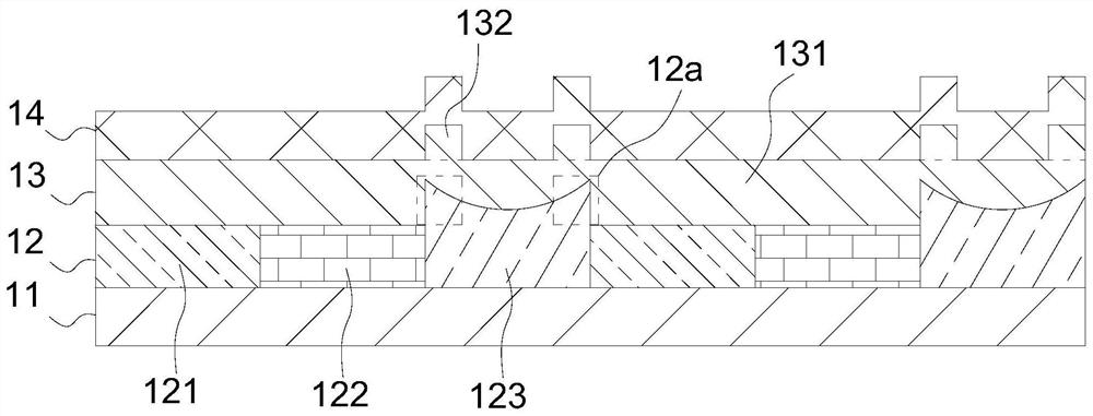
[0041] Please refer to figure 1 , figure 1 It is a structural schematic diagram of a preferred embodiment of the TFT array substrate of the present invention.

[0042] The TFT array substrate of the preferred embodiment of the present invention includes a TFT array layer 11 , a color filter layer 12 , a passivation layer 13 and a pixel electrode layer 14 .

[0043] Specifically, the color filter layer 12 is disposed on the TFT array layer 11, and includes a plurality of color-resist units, the plurality of color-resist units are respectively filled with red photoresist, green photoresist and blue photoresist, and correspondingly form a red photores...


PUM

PropertyMeasurementUnit
thicknessaaaaaaaaaa
transmittivityaaaaaaaaaa

Abstract

A TFT array substrate and a manufacturing method therefor. The TFT array substrate comprises a TFT array layer (11), a color filter layer (12), and a passivation layer (13). The color filter layer (12) comprises a blue subpixel (123), and the passivation layer (13) comprises a passivation layer body (131) and protruding parts (132) protruding from the passivation layer body (131). The protruding parts (132) of the passivation layer (13) are formed in regions on two sides of the blue subpixel (123) of the color filter layer (12), increasing the photoresistance of the regions on two sides of the blue subpixel (123) and making the thickness of the passivation layer (13) uniform, thus reducing differences in chromaticity.

Description

technical field [0001] The invention relates to the field of display technology, in particular to a TFT array substrate and a manufacturing method thereof. Background technique [0002] A liquid crystal display (Liquid Crystal Display, LCD) has many advantages such as a thin body, power saving, and no radiation, and has been widely used. Examples include LCD TVs, mobile phones, PDAs, computer screens, and laptop screens. [0003] Usually TFT-LCD (Thin Film Transistor Liquid Crystal Display) includes a color filter and a thin film transistor array substrate (TFT substrate) and a liquid crystal layer. Among them, the color filter provides R / G / B colors, and is currently made of photoresist. [0004] Due to the leveling problem of the photoresist, the sub-pixel pattern actually produced is concave (bowlshape), and the width of the depression exceeds 0.5 microns, resulting in a large difference in chromaticity between the center position and the edge position of the sub-pixel, ...

Claims


Application Information

Patent Timeline
Patent Type & Authority Patents(China)
IPC IPC(8): G02F1/1362G02F1/1368G02F1/1335H01L27/12H01L21/84
CPCG02F1/133514G02F1/1362G02F1/1368G02F1/136222G02F1/136295H01L27/1214H01L27/1259H01L27/1288
Inventor 李培宏宋江江
Owner WUHAN CHINA STAR OPTOELECTRONICS SEMICON DISPLAY TECH CO LTD
Why Eureka
Try Eureka