Method of growing electrical conductors

a technology of electrical conductors and growth methods, applied in the direction of chemical vapor deposition coatings, electrical equipment, coatings, etc., can solve the problems of difficult to attach source chemical molecules to the surface, difficult to deposit high-quality elemental metal thin films by ald type methods, and difficult to achieve high-quality metal thin films. , to achieve the effect of excellent step coverage and complicated thin film processing

Active Publication Date: 2006-06-27
ASM INTERNATIONAL
View PDF35 Cites 145 Cited by
  • Summary
  • Abstract
  • Description
  • Claims
  • Application Information

AI Technical Summary

Benefits of technology

[0043]Embodiments described herein provide methods of producing high quality conductive thin films with excellent step coverage, uniform thickness over a large area and excellent adhesion properties. The thin films may be used, for example, as seed layers for the electrodeposition of metal layers, as gate metals in thin film transistors and as capacitor electrodes for advanced high-density integrated circuits.
[0050]Certain embodiments described herein are especially beneficial for making electrically conductive layers in structures that have high aspect ratios, like vias, trenches, local high elevation areas and other similar surface structures that make the surface rough and complicate thin film processing by conventional CVD and PVD methods. An ALD metal oxide process combined with a reduction step provides excellent step coverage of electrically conductive thin films on all surface formations.

Problems solved by technology

However, due to the fact that ALD is based on sequential self-saturating surface reactions of source chemical compounds and utilization of active surface sites, depositing high quality elemental metal thin films by ALD is very difficult.
Usually the growth rate is well below one molecular layer / cycle because the adsorbed source chemical molecules may be bulky (steric hindrance) or because substrate temperature affects the number of active sites (e.g., —OH groups) on the surface.
In contrast to metal oxide films, experiments have revealed a drawback of the growth of metal thin films by an ALD type method.
In the case of metal deposition it is difficult to attach source chemical molecules to the surface because few active sites exist on the surface.
The metal film grown is often non-uniform over an area of the substrate and it is easily peeled off from the surface, which indicates very poor adhesion of the film to the substrate.
Reproducibility of such an ALD metal growth process has traditionally been poor and the reactions do not take place at all on insulating surfaces like silicon oxide.
Thus, the deposition time for a 10 nm copper seed layer would be over 5 hours, which is uneconomical for wafer processing.
With increasing aspect ratio it is becoming difficult to get sufficient step coverage for the seed layer with the state of the art technology.
These memory capacitors must be recharged frequently due to charge leakage.
Decreasing the distance between the conductors causes voltage breakdown when the insulator thickness is too thin to hold the voltage.
However, the aforementioned high-k dielectrics create new problems, since they donate oxygen to the conductor and thus the capacitor properties deteriorate.
But it is difficult to deposit thin films with good step coverage on new capacitor structures with small feature size and aggressive aspect ratio.
They used Ta2O5 as the capacitor dielectric while the electrodes consisted of ruthenium deposited by CVD from Ru(EtCp)2 and gaseous oxygen at 300–400° C. Problems related to the method included poor step coverage and reaction speed sensitivity.
The reaction of Ru(EtCp)2 with O2 was adversely affected by the partial pressures of the compounds.
However, several problems are associated with the use of poly-Si gate electrodes.
Poly-Si is thermodynamically unstable against high dielectric constant materials at high processing temperatures.
Refractory metals have been suggested for gate metals but the stability of the metal—gate oxide interface has been an issue.
However, appropriate methods of depositing high-quality platinum group metal thin films for gate electrode applications have not yet been developed.
However, they had problems with the quality of the nickel film: pinholes were formed on the thin films during the reduction of NiO with hydrogen gas.

Method used


Image

  • Method of growing electrical conductors
  • Method of growing electrical conductors
  • Method of growing electrical conductors

Examples


example 1

ALD of Cobalt Oxide

[0136]Co(thd)3 and O3 were used as source chemicals for the cobalt oxide deposition in an ALD reactor. Co(thd)3 was heated to 110° C. O3 was prepared from 99.9999% O2 with an external ozone generator. The resulting oxygen source gas mixture consisted of 10–20 vol.- % O3 in O2. Nitrogen, evaporated from liquid nitrogen, was used as an inert purging gas. Co(thd)3 pulse length varied from 1.5 s to 2.0 s, while O3 pulse (flow rate 100 std.cm3 / min) length varied from 2.0 s to 4.0 s. Silicon was used as the substrate material. Substrate temperatures between 150° C. and 350° C. were tested. One pulsing cycle consisted of four sequential steps: Co(thd)3 pulse, N2 purge, O3 pulse, N2 purge.

[0137]The higher deposition temperature tested resulted in uncontrolled film growth, as Co(thd)3 decomposed thermally thus producing a poor thickness profile for the thin film. At the lower substrate temperatures, a controlled growth rate of the thin film (0.3 Å / cycle) and good adhesion ...

example 2

ALD of Palladium Oxide

[0138]Substrates with Si, TiN, WN, W3C and SiO2 surfaces were loaded into an F-120 ALD reactor manufactured by ASM Microchemistry Ltd., Finland. Pd(thd)3 was loaded into a solid source tube of the reactor. The reactor was pumped to vacuum. The pressure of the reaction chamber was adjusted to about 5–10 mbar with flowing nitrogen gas while the pumping of the reactor continued. The Pd(thd)3 was heated to 110° C. and the reaction chamber to 150° C.

[0139]One pulsing cycle consisted of four steps in the following order: Pd(thd)3 pulse (2.0 s), N2 purge (1.0 s), O3 pulse (4.0 s), N2 purge (2.0 s).

[0140]The growth rate of palladium oxide from Pd(thd)3 and O3 was 0.15 Å / cycle at 150° C. According to EDS the film consisted of palladium oxide. The film grew on Si, TiN, WN, WC (tungsten carbide) and SiO2 surfaces and showed good adhesion.

example 3

Thermal Hydrogen as a Reducing Agent for the Reduction of ALD-grown Copper Oxide

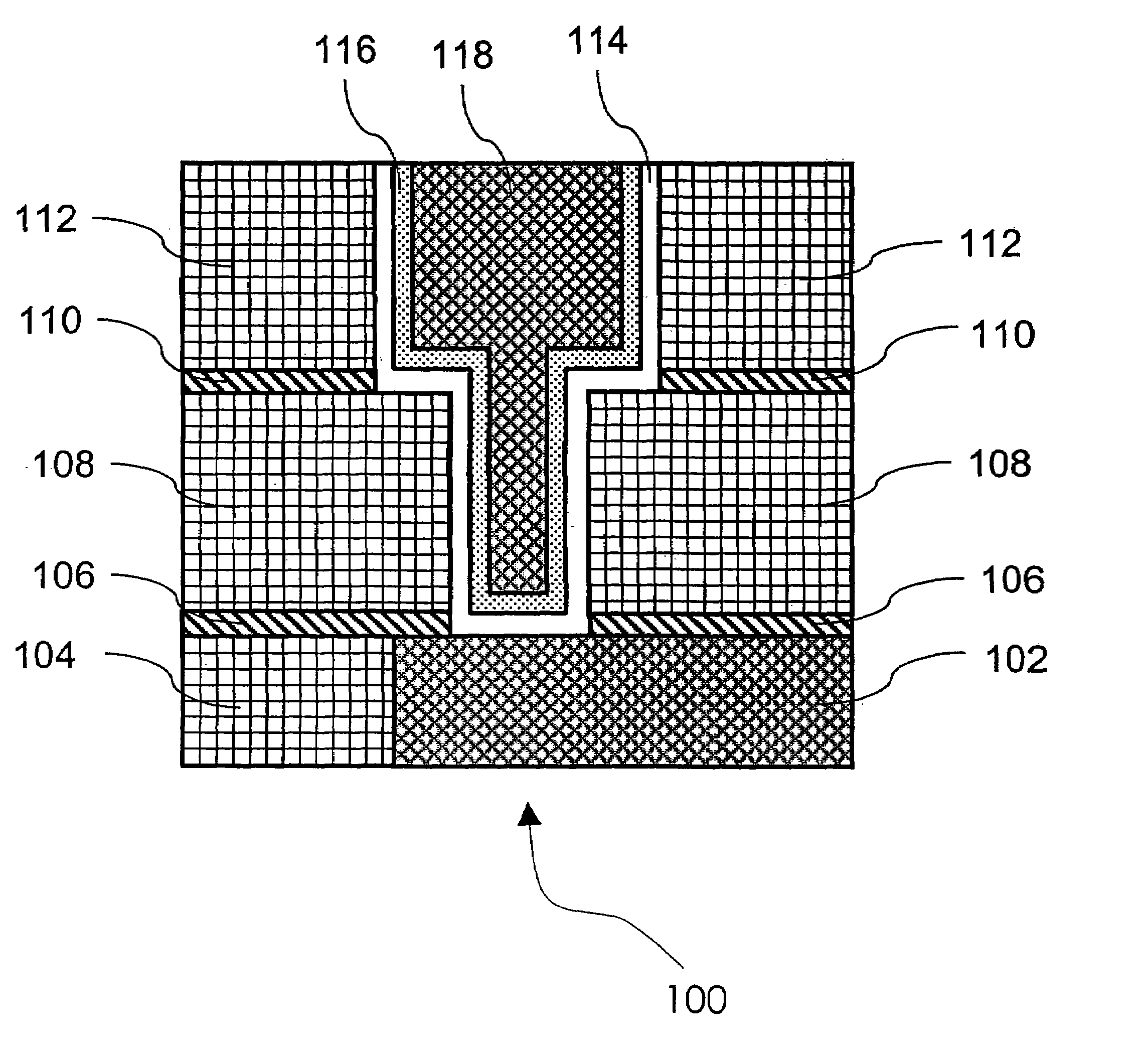
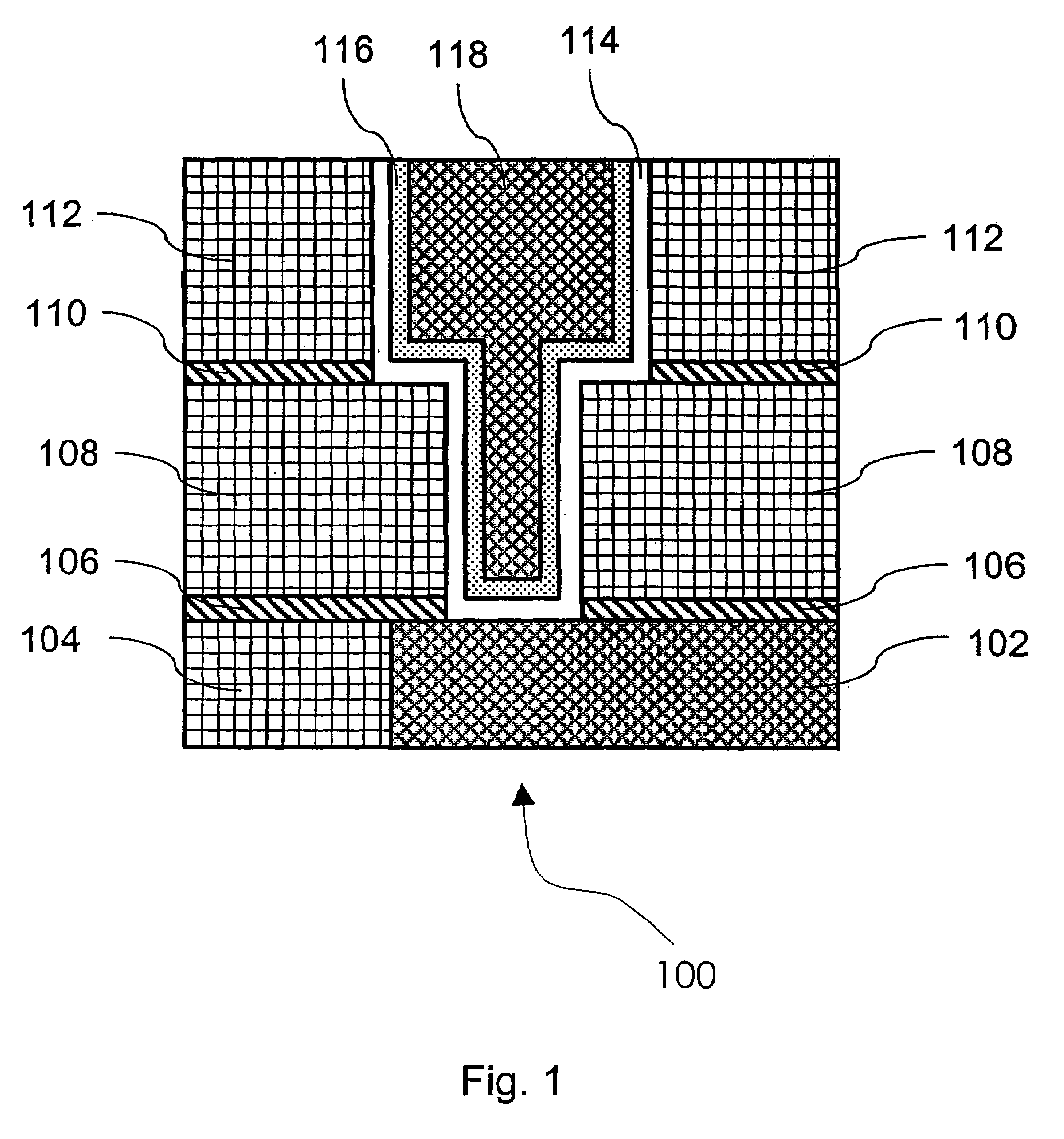
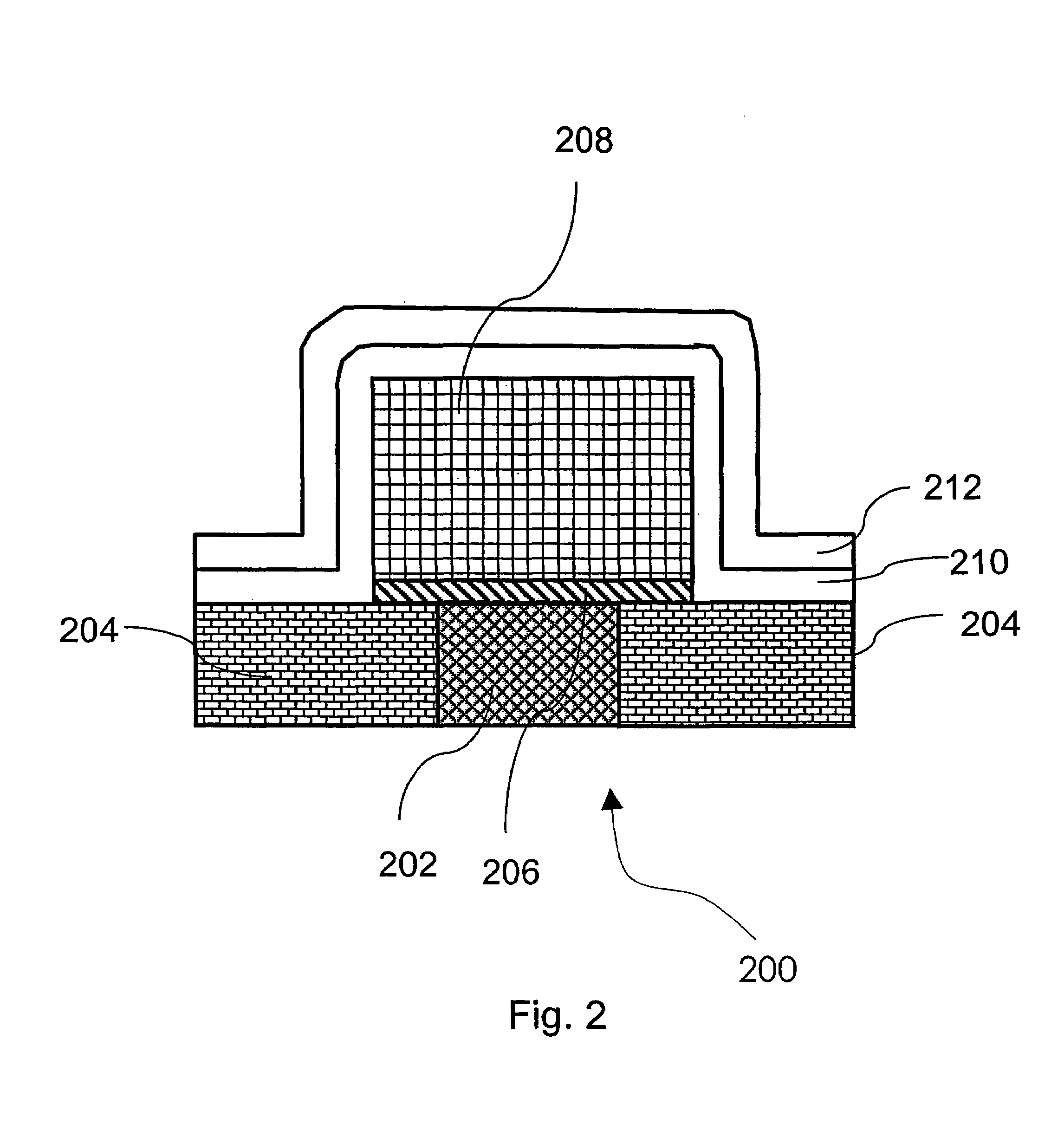
[0141]A silicon substrate having 20 nm of thermal silicon dioxide on the surface was loaded to the reaction space of a Pulsar® 2000 ALCVD™ reactor. The pressure of the reaction space was adjusted to about 1–20 mbar with a vacuum pump and flowing nitrogen gas (claimed purity 99.9999%). The temperature of the reaction space was adjusted to about 300–315° C. Tungsten nitride carbide (WNC) thin film was deposited on the thermal SiO2 from alternate pulses of WF6, NH3 and triethylboron (TEB). The deposition cycle consisted of WF6 pulse 0.25 s, N2 purge 1 s, NH3 pulse 0.75 s, N2 purge 1 s, TEB pulse 0.1 s and N2 purge 1 s. These pulse and purge times serve as examples of suitable values for the deposition process. Typically, pulse and purge times are selected from a range of about 0.05 s–3 s. Depending on the experiment, the deposition cycle was repeated 30–150 times, resulting in a WNC thin film having a thick...


PUM

PropertyMeasurementUnit
thickaaaaaaaaaa
thicknessaaaaaaaaaa
thicknessaaaaaaaaaa

Abstract

A method for forming a conductive thin film includes depositing a metal oxide thin film on a substrate by an atomic layer deposition (ALD) process. The method further includes at least partially reducing the metal oxide thin film by exposing the metal oxide thin film to a gaseous inorganic reducing agent, thereby forming a metal layer. In preferred arrangements, the reducing agent comprises of thermal hydrogen (H2), hydrogen radicals (H*) and / or carbon monoxide (CO).

Description

PRIORITY APPLICATION[0001]This application claims the benefit of U.S. Provisional Application 60 / 492,486, filed Aug. 4, 2003, the entire disclosure of which is incorporated by reference herein.FIELD OF THE INVENTION[0002]The present invention relates generally to the manufacturing of integrated circuits (ICs), and particularly to thin metal layers, such as for seed layers in damascene and dual damascene processes, gate metals of thin film transistors and capacitor electrodes in ICs.DESCRIPTION OF THE RELATED ART[0003]The atomic layer deposition (ALD) method of depositing thin films has several attractive features including excellent step coverage, even on large areas, and a dense and pinhole-free structure. Therefore, it is of great interest to apply ALD to the deposition of metallization layers of advanced integrated circuits (ICs), where the continuously increasing packing density and aspect ratio set higher and higher demands upon the metallization layers. Applications where high...

Claims


Application Information

Patent Timeline
Patent Type & Authority Patents(United States)
IPC IPC(8): H01L21/20C23C16/40C23C16/56H01L21/02H01L21/28H01L21/314H01L21/768H01L29/76
CPCC23C16/40H01L21/28079H01L21/3141H01L21/76823H01L21/76826H01L21/76828H01L21/76829H01L21/76832H01L21/76834H01L21/76843H01L21/76862H01L21/76873C23C16/56H01L28/65H01L21/28088H01L21/76807H01L21/0228
Inventor KOSTAMO, JUHANASTOKHOF, MAARTEN
Owner ASM INTERNATIONAL
Why Eureka
Try Eureka