Semiconductor light emitting device and vehicle lamp

a technology of light source, which is applied in the direction of fixed installation, light and heating apparatus, transportation and packaging, etc., can solve the problems of difficult to make the brightness distribution completely uniform, color unevenness occurring in mixed light, and intentionally making the brightness distribution over the light emitting surface non-uniform, etc., to reduce the amount of light, improve the use efficiency of light from the semiconductor light emitting device as a light source, and reduce the effect of chromaticity differen

Active Publication Date: 2016-01-26
STANLEY ELECTRIC CO LTD
View PDF35 Cites 0 Cited by
  • Summary
  • Abstract
  • Description
  • Claims
  • Application Information

AI Technical Summary

Benefits of technology

[0021]In the semiconductor light emitting device according to the one aspect of the present invention, the wavelength converting layer covering the light emitting surface of the semiconductor light emitting element has different wavelength conversion characteristics respectively at its portion covering the area of relatively high current density of the semiconductor light emitting element and at its portion covering the area of relatively low current density so as to reduce chromaticity difference occurring in the mixed light due to the non-uniform current density distribution at light emission operation in the semiconductor light emitting element, and hence even though the brightness distribution or emission wavelength distribution over the light emitting surface of the semiconductor light emitting element is non-uniform, the occurrence of color unevenness in mixed light can be suppressed. Thus, with the semiconductor light emitting device according to the present invention, a uniform emission color can be obtained with a desired brightness distribution being formed, and therefore the semiconductor light emitting device can be a light source suitable for use in, e.g., vehicle lamps.
[0022]In the vehicle lamp according to the other aspect of the present invention, the projection image is formed such that image parts corresponding to a part having a peak of brightness of the semiconductor light emitting device form a line along a cutoff line, and hence a light distribution pattern suitable for a passing-each-other beam can be formed with suppressing the amount of light cut off by a light-shielding member such as a shade to a minimum. Thus the use efficiency of light from the semiconductor light emitting device as a light source can be improved. Because the semiconductor light emitting device according to the present invention emits mixed light without color unevenness as described above, also with the vehicle lamp comprising this semiconductor light emitting device as a light source, a projection image without color unevenness can be generated.

Problems solved by technology

Meanwhile, in semiconductor light emitting devices used in vehicle lamps such as car headlights, the brightness distribution over the light emitting surface may be intentionally made to be non-uniform in order to efficiently obtain a desired light distribution pattern.
If a wavelength converting layer of a uniform thickness and concentration is formed on the light emitting surface of a light emitting element having such a non-uniform brightness distribution, the mixing ratio of light wavelength-converted by the wavelength converting layer to light passing through the wavelength converting layer without being wavelength-converted is different between low brightness areas and high brightness areas, resulting in color unevenness occurring in the mixed light.
Meanwhile, even in a light emitting element wherein electrodes and the like are placed so as to make the brightness distribution over the light emitting surface uniform, it is difficult to make the brightness distribution completely uniform, and thus the above problem of color unevenness may occur.
That is, in these years as light emitting elements are improving in quality and their application is widening, their brightness is becoming higher with the amount of current injected into the light emitting elements increasing, and accordingly the current density distribution inside the light emitting element and the brightness distribution over the light emitting surface are becoming likely to be non-uniform.
Hence, the high-low difference in the current density inside the light emitting element is increasing, and thus it is becoming more and more difficult to make the brightness distribution over the light emitting surface uniform, so that the way to deal with the above problem of color unevenness is becoming important.

Method used


Image

  • Semiconductor light emitting device and vehicle lamp
  • Semiconductor light emitting device and vehicle lamp
  • Semiconductor light emitting device and vehicle lamp

Examples


embodiment 1

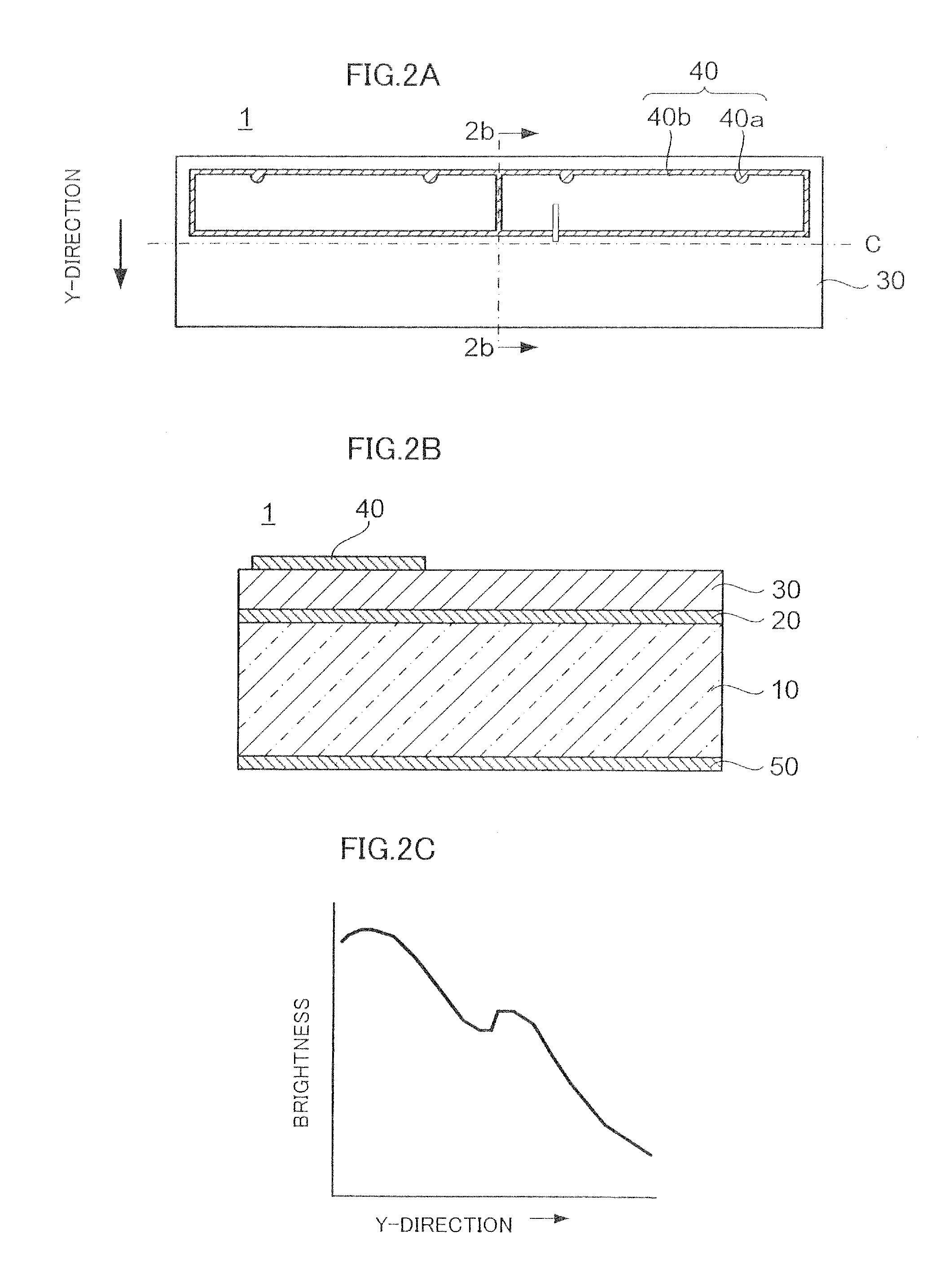
[0049]FIG. 2A is a plan view showing the configuration of a semiconductor light emitting element 1 according to an embodiment of the present invention, and FIG. 2B is a cross-sectional view taken along line 2b-2b in FIG. 2A. FIG. 2C is a graph showing the brightness distribution along the Y-direction in FIG. 2A of the semiconductor light emitting element 1. The semiconductor light emitting element 1 is a so-called thin-film structured light emitting element comprising a semiconductor film 30 and a support substrate 10 bonded together. Also, the semiconductor light emitting element 1 is a so-called vertically-structured light emitting element wherein a p-electrode 20 and an n-electrode 40 are placed opposite each other on opposite sides of the semiconductor film 30.

[0050]The support substrate 10 is made of, e.g., material of higher thermal conductivity (such as silicon or metal) than a growth substrate (not shown) used in the crystal growth of the semiconductor film 30. The p-electro...

embodiment 2

[0053]FIG. 4 is a cross-sectional view showing the structure of a semiconductor light emitting device 2b according to Embodiment 2 of the present invention, which is configured with a wavelength converting layer containing a fluorescent substance and laid over the surface (principal light emitting surface) of the above semiconductor light emitting element 1. The semiconductor light emitting device 2b has three wavelength converting layers 60a, 60b, 60c, which are different in the concentration of a fluorescent substance contained therein, on the surface of the semiconductor light emitting element 1. The three wavelength converting layers 60a, 60b, 60c have the concentrations of the fluorescent substance adjusted correspondingly to the non-uniform brightness distribution at light emission operation of the semiconductor light emitting element 1. Namely, the concentration of the fluorescent substance contained in the wavelength converting layer 60a, which covers the area of the highest...

embodiment 3

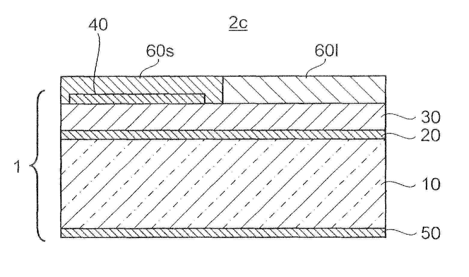
[0054]FIG. 5 is a cross-sectional view showing the structure of a semiconductor light emitting device 2c according to Embodiment 3 of the present invention, which is configured with a wavelength converting layer containing a fluorescent substance and laid over the surface of the above semiconductor light emitting element 1. In the semiconductor light emitting device 2c, wavelength converting layers 60s, 601, which contain fluorescent substances having different dominant wavelengths, are provided on the surface of the semiconductor light emitting element 1.

[0055]In the semiconductor light emitting element 1, the current density is high at the area over which the n-electrode 40 extends and low at the area over which the n-electrode 40 does not extend. Hence, the emission wavelength at the area over which the n-electrode 40 extends is shorter than the emission wavelength at the area over which the n-electrode 40 does not extend (blue shift). That is, the semiconductor light emitting el...


PUM


Abstract

A semiconductor light emitting device which produces mixed light of a desired emission color by a combination of a semiconductor light emitting element and a wavelength converting layer containing a fluorescent substance, and a vehicle lamp including the semiconductor light emitting device. The wavelength converting layer has different wavelength conversion characteristics respectively at its portion covering an area of relatively high current density at light emission operation of the semiconductor light emitting element and at its portion covering an area of relatively low current density so as to reduce chromaticity difference over the light extraction surface of the mixed light due to non-uniformity of current density in the light emitting layer at light emission operation.

Description

BACKGROUND OF THE INVENTION[0001]1. Field of the Invention[0002]The present invention relates to a semiconductor light emitting device including a semiconductor light emitting element such as an LED (light emitting diode), and a vehicle lamp comprising the semiconductor light emitting device.[0003]2. Description of the Related Art[0004]There have been known semiconductor light emitting devices which have a semiconductor light emitting element (hereinafter also called simply a light emitting element) that emits light having a specific wavelength when a current is injected and a fluorescent substance that absorbs part of light from the light emitting element to emit light having a wavelength longer than that of the light from the light emitting element in combination. With these semiconductor light emitting devices, light from the light emitting element and light from the fluorescent substance are mixed, so that mixed light of a desired emission color can be obtained.[0005]For example...

Claims


Application Information

Patent Timeline
Patent Type & Authority Patents(United States)
IPC IPC(8): H01L33/00H01L33/50F21S8/10
CPCH01L33/504F21S48/1154F21S48/1159H01L33/505H01L33/508F21S41/143F21S41/147F21S41/148H01L33/48H01L33/50
Inventor YOKOBAYASHI, YUSUKE
Owner STANLEY ELECTRIC CO LTD
Why Eureka
Try Eureka