Thin film transistor array substrate and manufacturing method of same

a technology of thin film transistors and array substrates, applied in the field of display technologies, can solve problems such as poor color of products, and achieve the effect of reducing chromaticity differences and reducing light transmittance loss

Inactive Publication Date: 2020-02-20
WUHAN CHINA STAR OPTOELECTRONICS SEMICON DISPLAY TECH CO LTD
View PDF1 Cites 0 Cited by
  • Summary
  • Abstract
  • Description
  • Claims
  • Application Information

AI Technical Summary

Benefits of technology

[0038]Compared with a TFT array substrate of the prior art, in the TFT array substrate and the manufacturing method of same of the embodiment of the present disclosure, by forming the protrusions of the passivation layer on the two side areas of the blue sub-pixel of the color filter layer, the photoresist on the two side areas of the blue sub-pixel is increased, such that a thickness of the passivation layer is uniformized, this reduces chromaticity difference. In addition, the protrusions can concentrate light scattered by the blue photoresist to reduce loss of light transmittance and solve the problem that a blue sub-pixel of a conventional TFT array substrate is in bowl shaped, and chromaticity difference between a center position and an edge position of the blue sub-pixel is too large, thereby affecting technical issues with product color.

Problems solved by technology

However, a specification of chromaticity difference is ±0.002, the recess of the sub-pixel leads to poor color of a product, among which the blue sub-pixel is most obvious.

Method used


Image

  • Thin film transistor array substrate and manufacturing method of same
  • Thin film transistor array substrate and manufacturing method of same
  • Thin film transistor array substrate and manufacturing method of same

Examples


Embodiment Construction

[0048]In the drawings, similar structural units are denoted by same reference numerals. The following description is based on the illustrated specific embodiments of this disclosure, which should not be construed as limiting other specific embodiments not discussed in detail herein.

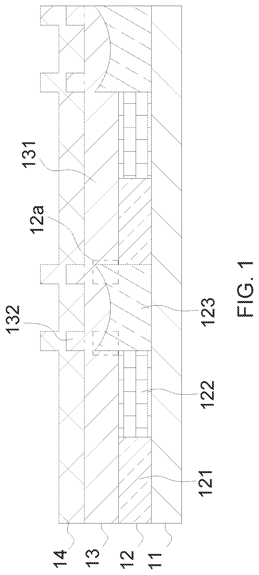
[0049]Refer to FIG. 1, a schematic structural view of a thin film transistor (TFT) array substrate according to an embodiment of the present disclosure is provided.

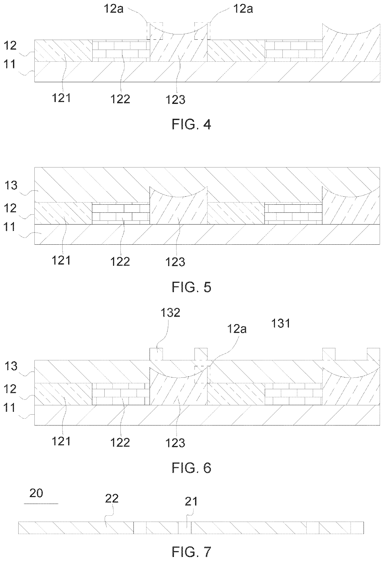
[0050]The TFT array substrate of the embodiment of the present disclosure includes a TFT array layer 11, a color filter layer 12, a passivation layer 13, and a pixel electrode layer 14.

[0051]In details, the color filter layer 12 is disposed on the TFT array layer 11, and includes a plurality of color resisting units. The color resisting units are filled with a red photoresist, a green photoresist, and a blue photoresist, respectively, and correspondingly form a red sub-pixel 121, a green sub-pixel 122, and a blue sub-pixel 123. A thickness of t...


PUM

PropertyMeasurementUnit
widthaaaaaaaaaa
widthaaaaaaaaaa
thicknessaaaaaaaaaa

Abstract

A thin film transistor (TFT) array substrate and a manufacturing method of same are provided. The TFT array substrate includes a TFT array layer, a color filter layer, and a passivation layer. The color filter layer includes a blue sub-pixel, and the passivation layer includes a passivation layer body and a plurality of protrusions protruding on the passivation layer body. By forming the protrusions of the passivation layer on two side areas of the blue sub-pixel of the color filter layer, a photoresist on the two side areas of the blue sub-pixel is increased, such that a thickness of the passivation layer is uniformized, this reduces chromaticity difference.

Description

FIELD OF INVENTION[0001]The present disclosure relates to the field of display technologies, and more particularly to a thin film transistor (TFT) array substrate and a manufacturing method of same.BACKGROUND OF INVENTION[0002]Liquid crystal displays (LCDs) have many advantages such as having a thin body, power saving, and no radiation, and have been widely used in, for example, LCD televisions (TVs), mobile phones, personal digital assistants (PDAs), computer screens, and laptop screens.[0003]A thin film transistor (TFT) LCD generally includes a color filter, a TFT array substrate, and a liquid crystal layer. The color filter provides red, green, blue colors and is currently formed using a photoresist.[0004]Because of leveling issues of the photoresist, a pattern of an actually fabricated sub-pixel is in bowl shaped, and a width of a recess of the sub-pixel exceeds 0.5 micrometer, such that chromaticity difference between a center position and an edge position of the blue sub-pixel...

Claims


Application Information

Patent Timeline
Patent Type & Authority Applications(United States)
IPC IPC(8): G02F1/1362G02F1/1333H01L27/12
CPCH01L27/1288G02F1/1362G02F1/133345G02F1/1368G02F2001/136222H01L27/1248G02F2001/136236G02F1/133357G02F1/136222G02F1/136236
Inventor LI, PEIHONGSONG, JIANGJIANG
Owner WUHAN CHINA STAR OPTOELECTRONICS SEMICON DISPLAY TECH CO LTD
Why Eureka
Try Eureka