Solid-state imaging apparatus

a technology of solid-state imaging and imaging apparatus, which is applied in the direction of electrical apparatus, semiconductor devices, radio frequency controlled devices, etc., can solve problems such as image quality degradation

Inactive Publication Date: 2009-10-15
CANON KK
View PDF6 Cites 82 Cited by
  • Summary
  • Abstract
  • Description
  • Claims
  • Application Information

AI Technical Summary

Problems solved by technology

As a result, the carriers accumulated in a carrier accumulation region leak toward the

Method used


Image

  • Solid-state imaging apparatus
  • Solid-state imaging apparatus
  • Solid-state imaging apparatus

Examples


first embodiment

[0029]The first embodiment is described with reference to FIGS. 1 to 5.

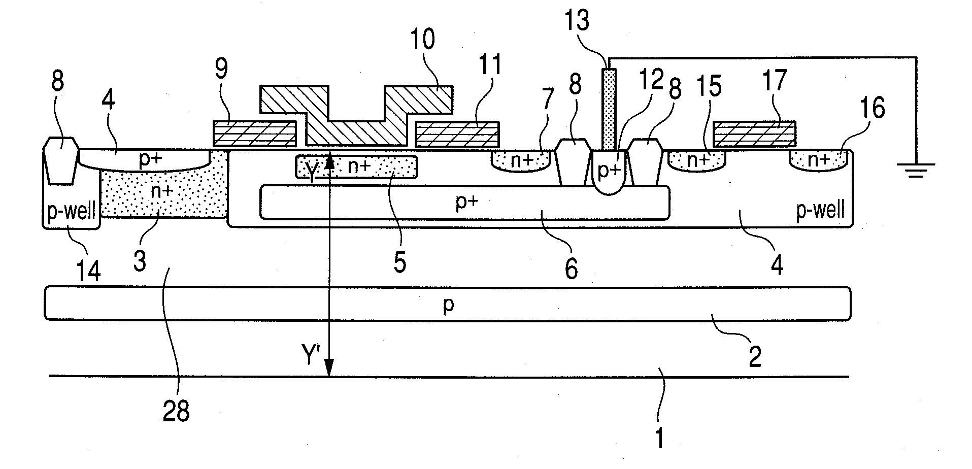
[0030]FIG. 1 is a schematic cross section of a solid-state imaging apparatus according to the present embodiment. The solid-state imaging apparatus includes an N-type semiconductor substrate 1 and a P-type semiconductor region (a fourth semiconductor region) 2 and the P-type semiconductor region 2 is called buried layer because it is buried deeply in a position below the surface of the substrate. The buried layer 2 extends between the semiconductor substrate 1 and an element arrangement surface region where a photoelectric conversion region and a carrier accumulation region are arranged and serves as a potential barrier against a signal carrier.

[0031]An N-type semiconductor region (a first semiconductor region) 3 and a P-type semiconductor region 4 form parts of the photoelectric conversion region respectively. The N-type semiconductor region 3 is a region (the same in polarity as the signal carrier) which is cap...

second embodiment

[0052]The second embodiment is described with reference to FIGS. 1, 2 and 6.

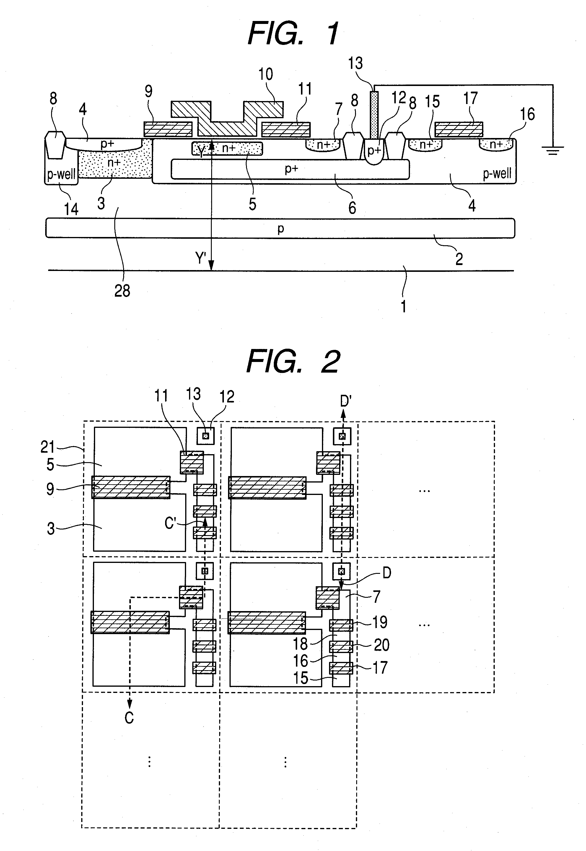
[0053]FIG. 6 is a cross section taken along with the line C-C′ of FIG. 2. The present embodiment is different from the first embodiment in that the potential barrier 6 is more extensive than the potential barrier 6 in the first embodiment, but the P well 14 is not arranged. Specifically, the potential barrier 6 is arranged under the FD region 7 and the source and the drain region 15 and 16 of the amplifying transistor. The potential barrier 6 may extend to under the source and the drain region of other MOS transistors. In such a configuration, if a potential on the source and the drain region of each MOS transistor varies during the operation of the VOFD function, a potential on the potential barrier 6 varies. However, the reference voltage is supplied to the potential barrier 6 through the P-type semiconductor region 12 to allow variation in potential to be reduced.

[0054]As is the case with the first embodi...

third embodiment

[0056]The third embodiment is described with reference to FIGS. 1, 2 and 7.

[0057]FIG. 7 is a cross section taken along with the line C-C′ of FIG. 2. The present embodiment is different from the first and the second embodiment in that a P-type semiconductor region 22 is further arranged under the P-type semiconductor region 6. FIG. 7 makes a description with reference to an example of configuration of the first embodiment. The P-type semiconductor region 22 is lower in impurity concentration than the potential barrier 6. A potential on the buried layer 2 is fixed at the outer periphery outside the pixel region.

[0058]In a case where the N-type semiconductor region 28 is arranged between the buried layer 2 and the potential barrier 6 like FIG. 1 to operate the VOFD, variation in potential on the buried layer 2 is prevented from being transferred to the potential barrier 6 due to capacitive coupling between the buried layer 2 and the potential barrier 6.

[0059]If any variation in potenti...


PUM


Abstract

A solid-state imaging apparatus, controlling a potential on a semiconductor substrate for an electronic shutter operation, includes: a first semiconductor region of the first conductivity type for forming a photoelectric conversion region; a second semiconductor region of the first conductivity type, formed separately from the photoelectric conversion region, for accumulating carriers; a third semiconductor region of a second conductivity type arranged under the second semiconductor region, for operating as a potential barrier; a fourth semiconductor region of the second conductivity type extending between the first semiconductor region and the semiconductor substrate, and between the third semiconductor region and the semiconductor substrate; and a first voltage supply portion for supplying a voltage to the third semiconductor region; wherein the first voltage supply portion includes a fifth semiconductor region of the second conductivity type arranged in the pixel region, and a first electrode connected to the fifth semiconductor region.

Description

BACKGROUND OF THE INVENTION[0001]1. Field of the Invention[0002]The present invention relates to a solid-state imaging apparatus with an electronic shutter function and, in particular, to a solid-state imaging apparatus which discharges a carrier toward a substrate.[0003]2. Description of the Related Art[0004]Hitherto, a solid-state imaging apparatus has used a so-called a vertical overflow drain (VOFD) in which a voltage is applied to a semiconductor substrate to discharge a carrier of a photoelectric conversion element to control accumulation time, thereby realizing an electronic shutter function. Particularly, the function is often used in a CCD solid-state imaging apparatus.[0005]Japanese Patent Application Laid-Open No. 2005-166731 proposes a solid-state imaging apparatus which causes a MOS solid-state imaging apparatus to operate a VOFD function to realize an electronic shutter function.[0006]A structure shown in Japanese Patent Application Laid-Open No. 2005-166731 leaves roo...

Claims


Application Information

Patent Timeline
IPC IPC(8): H01L27/148
CPCH01L27/14603H01L27/14609H01L27/1463H04N25/771H01L31/0224
Inventor KOBAYASHI, MASAHIROYAMASHITA, YUICHIRO
Owner CANON KK
Why Eureka
Try Eureka