Thermocouple

a thermocouple and sensor technology, applied in the field of thermocouples, can solve the problems of affecting the uniformity of the resulting structure on the surface of the substrate, the inability to use the surface of the finished substrate, and the failure of the thermocouple employed in measuring the temperature within the high-temperature processing chamber

Active Publication Date: 2009-12-17
ASM IP HLDG BV
View PDF60 Cites 312 Cited by
  • Summary
  • Abstract
  • Description
  • Claims
  • Application Information

AI Technical Summary

Benefits of technology

[0007]In one aspect of the present invention, a thermocouple for use in a semiconductor processing reactor is provided. The thermocouple includes a sheath having a measuring tip an end thereof. The thermocouple further includes a support member disposed within the sheath, and the support member has at least two bores fo...

Problems solved by technology

If the temperature varies greatly across the surface of the substrate, the deposited layer could be uneven which may result in unusable areas on the surface of the finished substrate.
Similarly, non-uniformity or instability of temperatures across a substrate during other thermal treatments can affect the uniformity of resulting structures on the surface of the substrate.
However, thermocouples employed in measuring the temperature within the high-temp...

Method used


Image

  • Thermocouple
  • Thermocouple
  • Thermocouple

Examples


Embodiment Construction

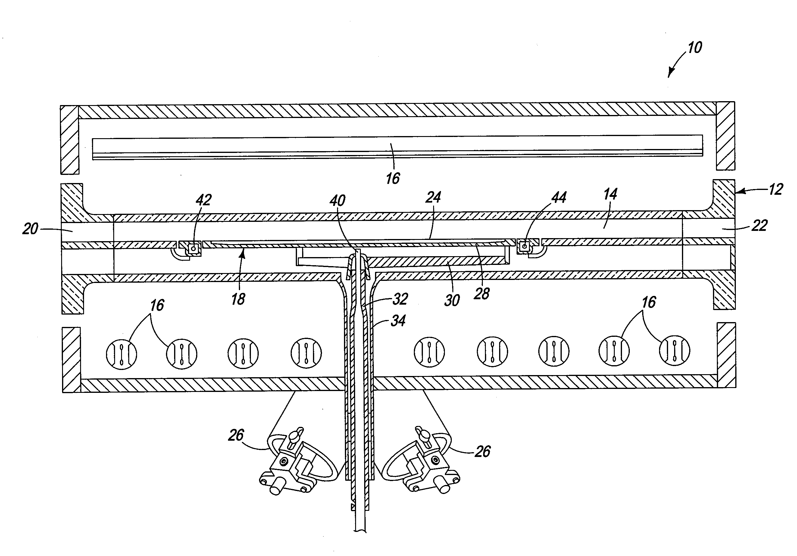
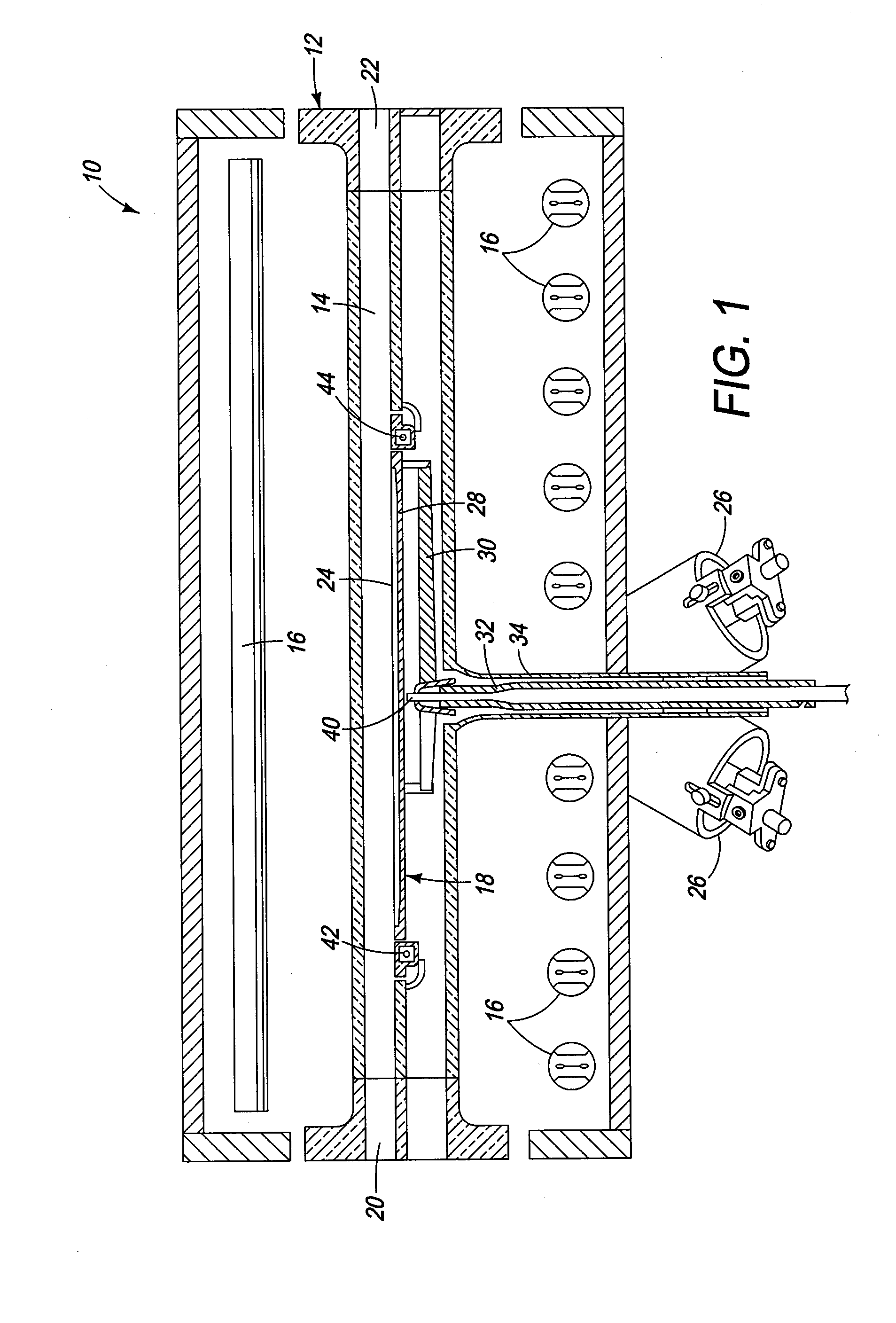
[0026]Referring to FIG. 1, an exemplary embodiment of a chemical vapor deposition (“CVD”) reactor 10 is shown. While the illustrated embodiment is a single substrate, horizontal flow, cold-wall reactor, it should be understood by one skilled in the art that the thermocouple technology described herein may be used in other types of semiconductor processing reactors as well as other applications requiring accurate temperature sensors. The reactor 10 includes a reaction chamber 12 defining a reaction space 14, radiant heating elements 16 located on opposing sides of the reaction chamber 12, and a substrate support mechanism 18. The reaction chamber 12 is an elongated member having an inlet 20 for allowing reactant gases to flow into the reaction space 14 and an outlet 22 through which the reactant gases and process by-products exit the reaction space 14. In an embodiment, the reaction chamber 12 is formed of transparent quartz. It should be understood by one skilled in the art that the...


PUM


Abstract

A thermocouple for use in a semiconductor processing reactor is described. The thermocouple includes a sheath having a measuring tip at one end and an opening at the other end. A support member having bores formed along the length is disposed within the sheath. A pair of wires formed of dissimilar metals are disposed within the bores, and one end of the wires is fused together to form a junction. The wires extend along the length of the bores. As the wires exit the bore, they are spatially or physically separated to prevent a short circuit therebetween. The ends of the wires exiting the bore are also free to thermally expand in the longitudinal manner, thereby reducing or eliminating the potential for the wires to fail due to grain slip.

Description

FIELD OF THE INVENTION[0001]The present invention relates to a temperature sensor, and more particularly to a temperature sensor configured to enhance accuracy of temperature control in a semiconductor processing apparatus.BACKGROUND OF THE INVENTION[0002]High-temperature semiconductor processing chambers are used for depositing various material layers onto a substrate surface or surfaces. One or more substrates or workpieces, such as silicon wafers, are placed on a workpiece support within the processing chamber. Both the substrate and workpiece support are heated to a desired temperature. In a typical processing step, reactant gases are passed over each heated substrate, whereby a chemical vapor deposition (CVD) reaction deposits a thin layer of the reactant material in the reactant gases on the substrate surface(s). Through subsequent processes, these layers are made into integrated circuits, and tens to thousands or even millions of integrated devices, depending on the size of t...

Claims


Application Information

Patent Timeline
IPC IPC(8): H01L35/02
CPCG01K13/00G01K7/04
Inventor YEDNAK, III, ANDY MICHAEL
Owner ASM IP HLDG BV
Why Eureka
Try Eureka