
CPU and memory connection assembly to extend memory address space

a technology of memory address space and assembly, which is applied in the direction of memory architecture accessing/allocation, instruments, computing, etc., can solve the problem that the entire memory space cannot be used, and achieve the effect of reducing the design period and reducing the design cos

Inactive Publication Date: 2009-12-31
SDCMICRO
View PDF2 Cites 19 Cited by
  • Summary
  • Abstract
  • Description
  • Claims
  • Application Information

AI Technical Summary

Benefits of technology

[0010]According to the present invention, two components are added to a memory IC chip such that a storage memory with capacity exceeding memory capacity of address pins of the CPU may be used. Therefore, a designing period for the entire system is reduced and the design cost is also reduced.

Problems solved by technology

When the number of address pins is less than memory capacity, entire memory space cannot be used due to the limited number of accessible memory addresses.

Method used


Image

  • CPU and memory connection assembly to extend memory address space
  • CPU and memory connection assembly to extend memory address space

Examples


Embodiment Construction

[0013]Hereinafter, a CPU and memory connection assembly according to an embodiment of the present invention will be described in detail with accompanying drawings.

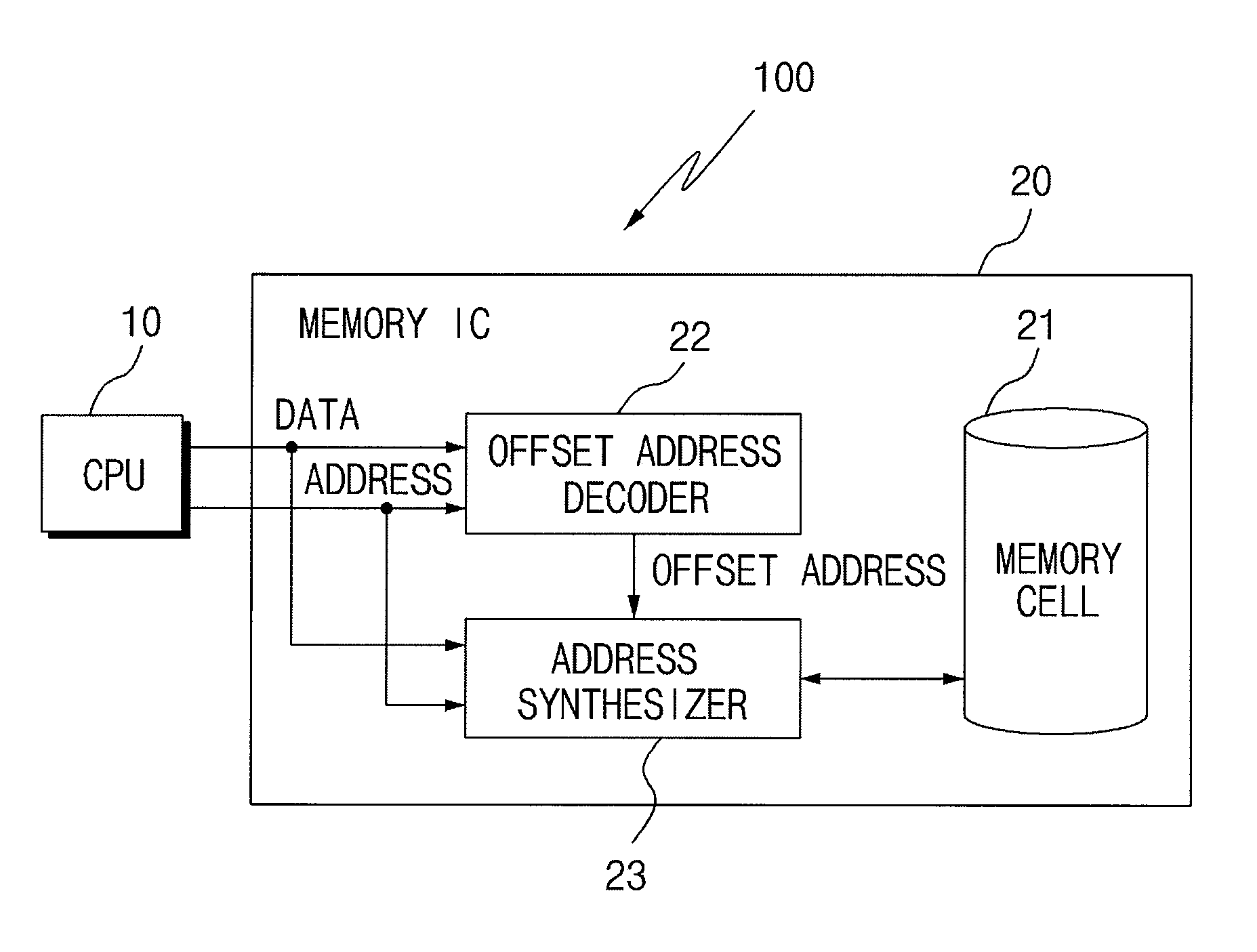
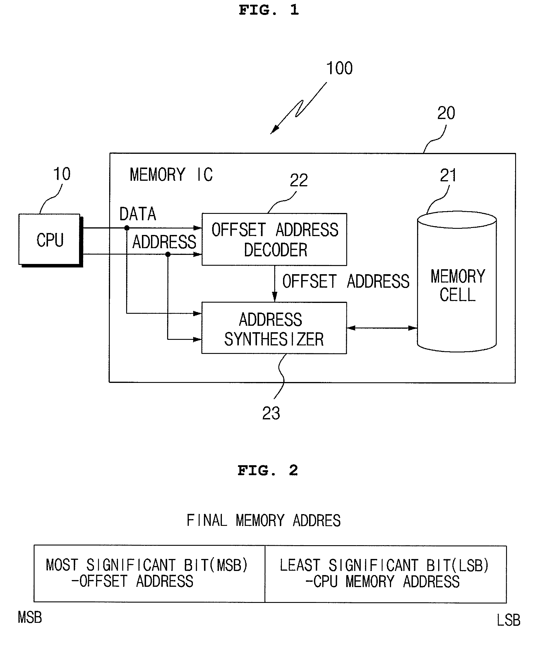
[0014]FIG. 1 is a block diagram illustrating a CPU and memory connection assembly according to an embodiment of the present invention. FIG. 2 is a view illustrating a result of a generated final memory address according to the embodiment of the present invention.

[0015]Referring to the drawings, a CPU and memory connection assembly 100 according to an embodiment of the present invention includes a CPU 10 generating and transmitting memory addresses and data to a memory IC chip 20 to be connected thereto for communication; and the memory IC chip 20 reading a memory address from which stored data is read from the CPU 10 and data to generate a final memory address to access a memory cell 21 that is provided in the memory IC chip 20. The memory IC chip 20 includes an offset address decoder 22 storing an offset address, which is...


PUM


Abstract

Disclosed is a CPU and memory connection assembly to extend memory address space without extending address pins. The CPU and memory connection assembly extends entire accessible memory address of a CPU using a small number of address pins by synthesizing a final memory address by receiving an offset address setting command inputted from a CPU through an offset address decoder to generate an offset address and by receiving CPU max address bit setting command directly inputted from the CPU through an address synthesizer to combine the CPU max address bit setting command with the address directly inputted from the CPU.

Description

BACKGROUND OF THE INVENTION[0001]1. Field of the Invention[0002]The present invention relates to a CPU and memory connection assembly to extend memory address space without extending address pins, and more particularly to, a CPU and memory connection assembly for extending entire accessible memory address of a CPU using a small number of address pins by synthesizing a final memory address by receiving an offset address setting command inputted from a CPU through an offset address decoder to generate an offset address and by receiving CPU max address bit setting command directly inputted from the CPU through an address synthesizer to combine the CPU max address bit setting command with the address directly inputted from the CPU.[0003]2. Description of the Related Art[0004]A NOR flash memory generally has address pins corresponding to memory capacity. To access the NOR flash memory, the CPU inputs a memory address to the address pins, and then reads or writes data at the memory addres...

Claims


Application Information

Patent Timeline
IPC IPC(8): G06F12/00
CPCG06F12/0623G06F2212/2022G06F2212/1004G06F13/10G06F13/14
Inventor LEE, JOO-HYEONGLEE, JAE-YONG
Owner SDCMICRO
Learn More