Isolation for multi-single-wafer processing apparatus

a processing apparatus and single-single-wafer technology, applied in the direction of chemical vapor deposition coating, metal material coating process, coating, etc., can solve the problems of compromising the design intent of non-contact isolation, not allowing a minimal reaction space volume, and difficult to maintain the tolerances required in the tig design

Inactive Publication Date: 2010-01-21
AIXTRON INC
View PDF18 Cites 223 Cited by
  • Summary
  • Abstract
  • Description
  • Claims
  • Application Information

AI Technical Summary

Benefits of technology

[0010]Various embodiments of an MSW processing apparatus are herein provided. In some embodiments, the MSW processing apparatus may include two or more semi-isolated reaction chambers and a separate indexer volume. The reaction chambers may be separated from one another by isolation regions configured with two or more TIG elements...

Problems solved by technology

This staircase-TIG design also addresses mechanical thermal expansion issues (dominated by radial expansion) that may otherwise make the tolerances required in a TIG design difficult to practically maintain.
The design also does not permit a minimal reaction space volume.
However, a serious drawback of these proposals is that thermal radial expansion of the different reactors—referenced to the center of the processing system—can result in contact across a vertical gap in each of these isolation areas, compromising a design intent on non-contact isolation.
In both such implementations th...

Method used


Image

  • Isolation for multi-single-wafer processing apparatus
  • Isolation for multi-single-wafer processing apparatus
  • Isolation for multi-single-wafer processing apparatus

Examples


Embodiment Construction

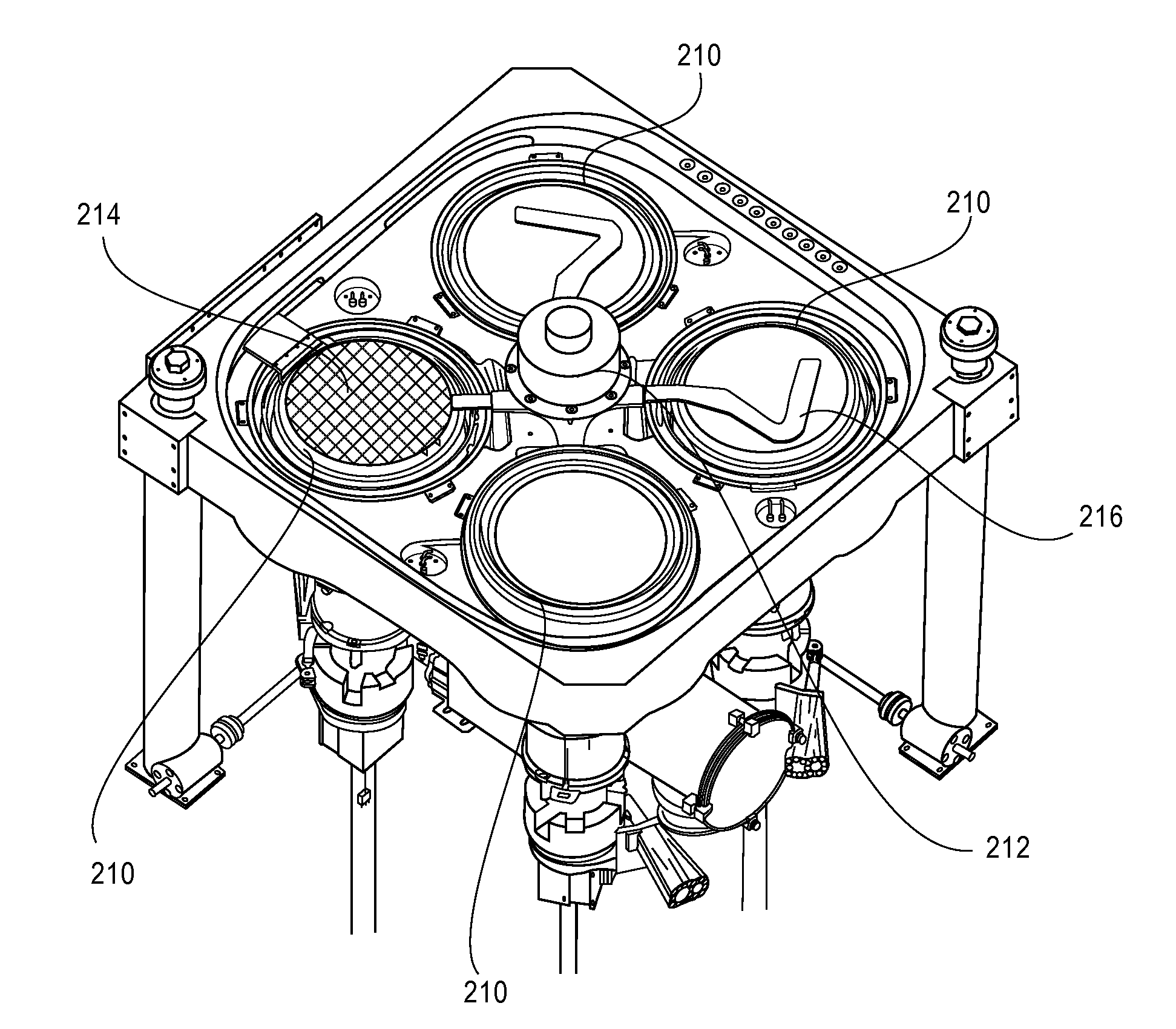
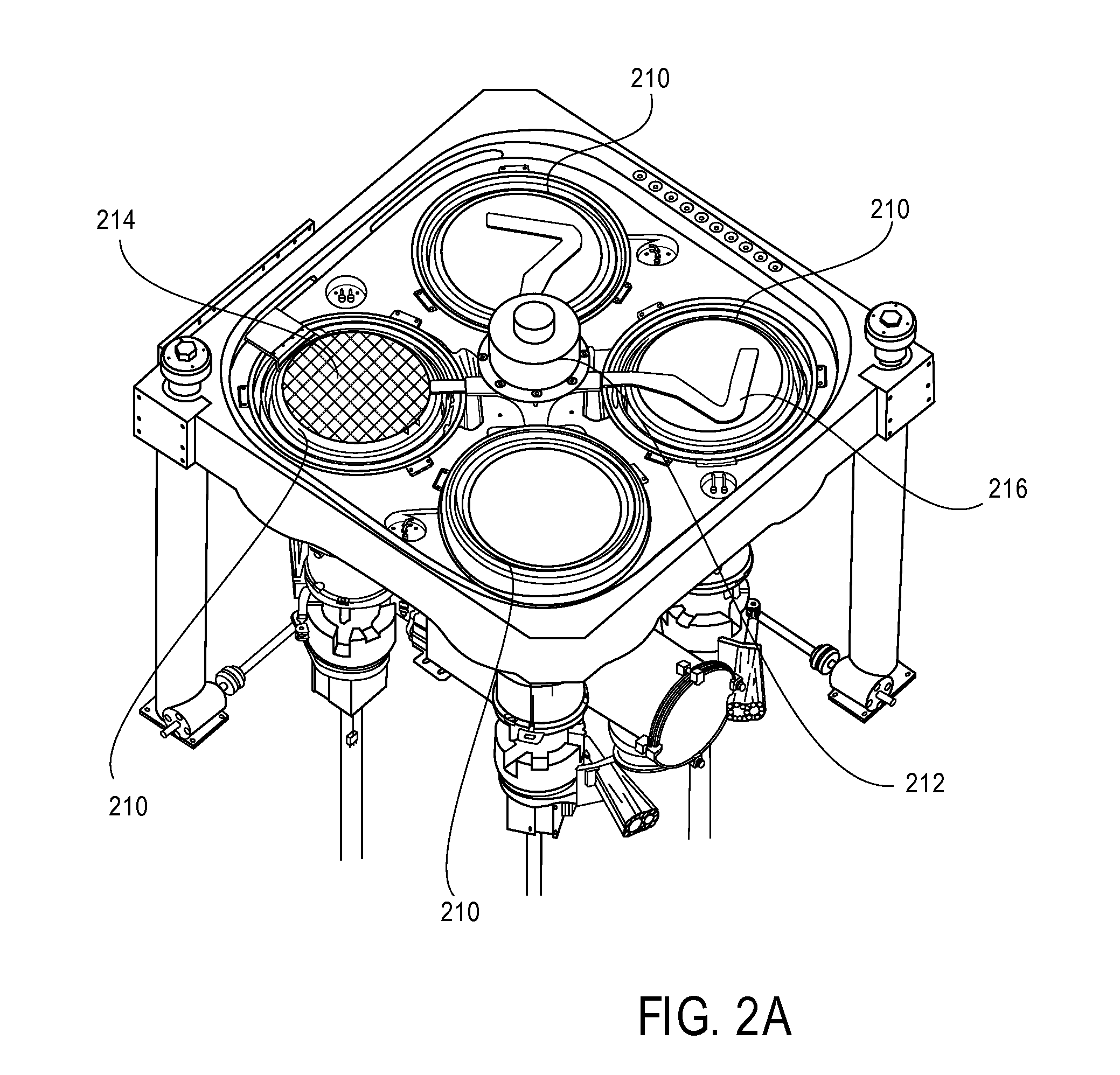
[0030]The present invention relates to methods and systems for providing isolation between reaction spaces or chambers within a multi-chamber processing unit of a semiconductor wafer processing station or similar apparatus. In one embodiment, the invention provides a high productivity, MSW processing apparatus suitable for cyclic deposition processes such as atomic layer deposition (ALD) and pulsed chemical vapor deposition (CVD) and including two or more semi-isolated reactors. In one instance, four such reactors are positioned radially about a common center and wafers are loaded by an indexer within a semi-isolated space in the process module housing the four reactors. These reaction chambers may be used for common deposition processes on wafers housed therein.

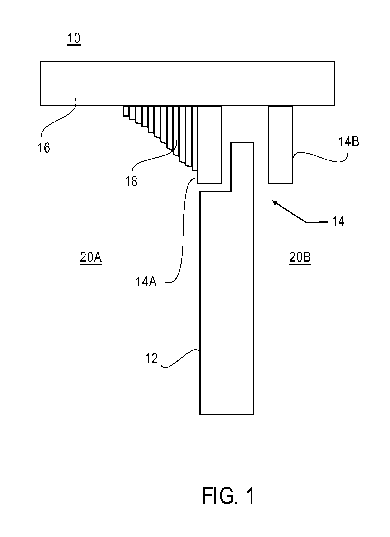
[0031]In order to obtain the state of semi-isolation between reaction chambers, each reaction chamber is configured with two or more TIG elements, at least one of which has a conformal staircase design, and either or both of...


PUM

PropertyMeasurementUnit
Temperatureaaaaaaaaaa
Timeaaaaaaaaaa
Volumeaaaaaaaaaa

Abstract

An MSW processing apparatus includes two or more semi-isolated reaction chambers separated from one another by isolation regions configured with two or more TIG elements, either or both of which may be independently purged. The TIG elements may be configured in a staircase-like fashion and include vertical and horizontal conductance spacings, sized so that, under different operational process temperatures of the MSW processing apparatus, a change in the horizontal conductance spacing is less than a change in the vertical conductance spacing.

Description

CROSS-REFERENCE TO RELATED APPLICATIONS[0001]This application is a non-provisional of, claims priority to, and incorporates by reference U.S. Provisional Patent Application 61 / 080,224, filed 11 Jul. 2008.BACKGROUND OF THE INVENTION[0002]The present invention relates to methods and systems for providing isolation between reaction spaces or chambers within a multi-chamber processing unit of a semiconductor wafer processing station or similar apparatus.[0003]U.S. patent application Ser. No. 11 / 780,698 and International Application PCT / US06 / 61201, each of which is assigned to a common owner of the present invention and incorporated herein by reference, describe wafer processing apparatus having multiple single wafer reaction chambers, one or more of which contain a vertically moveable heater-susceptor with an attached, annular flow ring conduit at its perimeter. The annular flow ring conduit has an external surface at its edge that isolates the outer space of the reaction chamber above ...

Claims


Application Information

Patent Timeline
IPC IPC(8): C23C16/46C23C16/00
CPCC23C16/45544C23C16/4409
Inventor SILVA, HUGODAUELSBERG, MARTINLINDNER, JOHANNESSEIDEL, THOMAS E.STRAUCH, GERHARD K.
Owner AIXTRON INC
Why Eureka
Try Eureka