Fine-pitch oblong solder connections for stacking multi-chip packages

a technology of multi-chip packages and solder connections, which is applied in the direction of semiconductor devices, semiconductor/solid-state device details, electrical apparatus, etc., can solve the problems of time-consuming, incompatible with the market requirements of low fabrication cost, and disruptive microcracks in metal fillings, so as to reduce the risk of device warpage, improve performance, and reduce the effect of manufacturing cos

Inactive Publication Date: 2010-03-25
TEXAS INSTR INC
View PDF4 Cites 63 Cited by
  • Summary
  • Abstract
  • Description
  • Claims
  • Application Information

AI Technical Summary

Benefits of technology

[0012]It is a technical advantage of the invention that the fabrication method of the PoP bottom device, including the step of encapsulating the top side in molding compound, proceeds in wafer form; the singulation into discrete devices by sawing is the last process step. As a result, the molding step provides each discrete device with a maximum amount of the robust molding material, contributing significantly to minimize any device warpage during the temperature excursion for assembling the PoP.
[0013]It is another technical advantage of the invention that the process step of opening the vias for exposing the device terminals proceeds through the whole thickness of the molded material and further creates smooth via sidewalls. As a result, the formation of any sidewall protrus...

Problems solved by technology

Further, applicant discovered that, for the bottom packages, the method of opening windows into the molding compound to expose solder bumps creates rough, un-even via sidewalls at the bump interface so that in the subsequent solder reflow cycle thermomechanical stresses are created between sidewalls and solder, which may lead ...

Method used


Image

  • Fine-pitch oblong solder connections for stacking multi-chip packages
  • Fine-pitch oblong solder connections for stacking multi-chip packages
  • Fine-pitch oblong solder connections for stacking multi-chip packages

Examples


Embodiment Construction

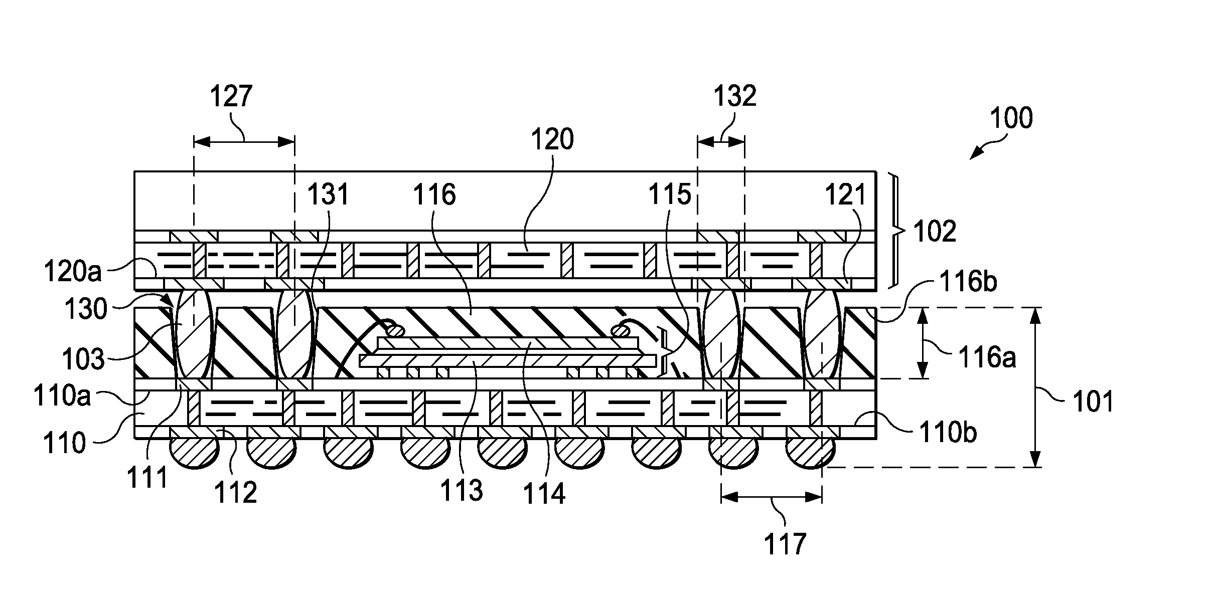
[0027]FIG. 1 illustrates an exemplary package-on-package (PoP) device, generally designated 100, according to an embodiment of the invention. PoP device 100 includes a first packaged device 101, a second packaged device 102, and solder bodies 103 connecting devices 101 and 102 electrically and mechanically.

[0028]First device 101 includes a first substrate 110, which is made of an insulating material yet integral with conductive lines and vias. First substrate 110 has a first side 110a and a second side 110b. On first side 110a are first contact pads 111, and on second side 110b are second contact pads 112. Second device 102 includes a second substrate 120, which is made of an insulating material yet integral with conductive lines and vias. Second substrate 120 has a third side 120a, which is oriented to face first device 101. On third side 120a are third contact pads 121.

[0029]In the area of substrate 110 is divided into a region, preferably in the approximate center of the of the s...


PUM


Abstract

A semiconductor PoP device (100) includes a first device (101) with a first substrate (110) having on its first side (110a) a stack (115) of at least two chips, first contact pads (111), and a first package (116) having a height (116a) and a top surface (116b). Via holes (130) extend from the top package surface through the package height to the first contact pads; the vias have straight sidewalls and a diameter at the top surface of less than 75% of the height. The PoP further includes a second packaged device (102) with a second substrate (120) facing the top surface (116b) of the first package; substrate (120) has contact pads (121) in line with the first pads (111). Solder bodies (103) fill the vias (130) and connect the pads (121) with the respective first pads (111). In the fabrication method of first device (101), the vias (130) are opened through the complete package thickness (116a); thereafter, enough solder balls are filled into each via to insure contact with the respective solder body attached to the second package.

Description

FIELD OF THE INVENTION[0001]The present invention is related in general to the field of semiconductor devices and processes and more specifically to the structure and fabrication method of vertically integrated low-profile, fine-pitch package-on-package integrated circuit assemblies having oblong solder connections.DESCRIPTION OF RELATED ART[0002]A package-on-package (PoP) device in semiconductor technology is created by aligning a top device package with a bottom device package, and connecting the output terminals of the top package with the input terminals of the bottom package. The connection of terminals is achieved by reflowing the solder body attached to each output terminal to wet the respective terminal of the bottom package. In today's semiconductor products, PoP devices enjoy increasing popularity, because they promise to use component devices already developed and thus quickly available. For instance, examples for mobile multimedia applications include the three-dimension...

Claims


Application Information

Patent Timeline
IPC IPC(8): H01L25/065H01L23/48H01L21/50H01L21/78
CPCH01L21/561H01L2924/3511H01L24/97H01L25/105H01L2224/16225H01L2224/48091H01L2224/48227H01L2224/73265H01L2224/97H01L2225/06558H01L2924/01082H01L2924/14H01L2924/1433H01L2924/15331H01L23/3128H01L2924/1815H01L2224/48465H01L2224/32145H01L2924/01033H01L2924/01006H01L2225/1058H01L2225/1023H01L24/48H01L2924/00014H01L2224/85H01L2224/81H01L2924/00H01L2924/00012H01L24/73H01L2224/04042H01L2924/181H01L2224/45099H01L2224/45015H01L2924/207
Inventor GERBER, MARK A.
Owner TEXAS INSTR INC
Why Eureka
Try Eureka