Method for exposing and cleaning insulating coats from metal contact surfaces

a technology of metal contact surface and insulating coating, which is applied in the direction of chemistry apparatus and processes, basic electric elements, light and heating apparatus, etc., can solve the problems of inability to deliver the required high assembly yield and reliability test data, inability to reliably contact the solder of the top device, and unacceptably high number of open contact failures between the solder balls, etc., to achieve the effect of reducing device warpage and increasing performan

Active Publication Date: 2013-04-30
TEXAS INSTR INC
View PDF1 Cites 1 Cited by
  • Summary
  • Abstract
  • Description
  • Claims
  • Application Information

AI Technical Summary

Benefits of technology

[0009]It is a technical advantage of the invention that the fabrication method of the PoP bottom device, including the step of encapsulating the top side in molding compound, may proceed in strip form; the singulation into discrete devices by sawing becomes the last process step. As a result, the molding step provides each discrete device with a maximum amount of the robust molding material, contributing significantly to minimize any device warpage during the temperature excursion for assembling the PoP.
[0010]It is another technical advantage that the break-up of glassy coats by the vapor pressure of flux fumes is applicable to any metal surface originally covered by the overmolding compound, for example solder and gold-clad copper.
[0011]In another technical advantage of the invention, the overmolded bottom device may include one or more wire-bonded chips, giving the PoP the advantage of using existing chips for increased performance.

Problems solved by technology

Applicants recognized that the PoP approach of packaging the bottom device in an overmolding compound including inorganic filler particles, and then opening the apertures with lasers to expose the contact pads lends itself to higher I / O's numbers and finer pitch, but that this approach, until now, did not deliver the needed high assembly yield and reliability test data.
Significantly, unacceptably high numbers of open contact failures have been observed between the solder balls of the top device and the metal contact of the bottom device, both for bottom devices fabricated with gold-clad copper contact pads and for bottom devices fabricated with solder balls on the pads.
As a consequence, the glassy coats tend to remain on the surface of both solder and gold contacts and inhibit reliable contact with the solder of the top device.

Method used


Image

  • Method for exposing and cleaning insulating coats from metal contact surfaces
  • Method for exposing and cleaning insulating coats from metal contact surfaces
  • Method for exposing and cleaning insulating coats from metal contact surfaces

Examples


Embodiment Construction

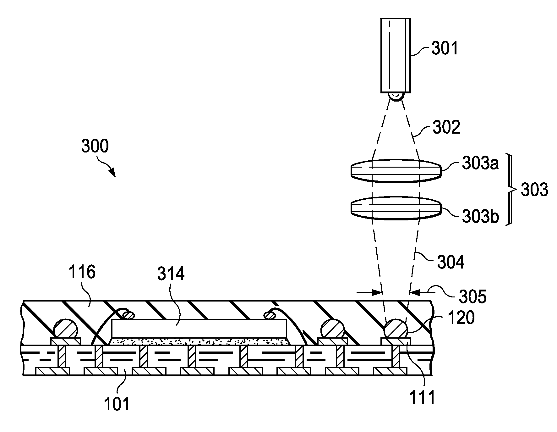
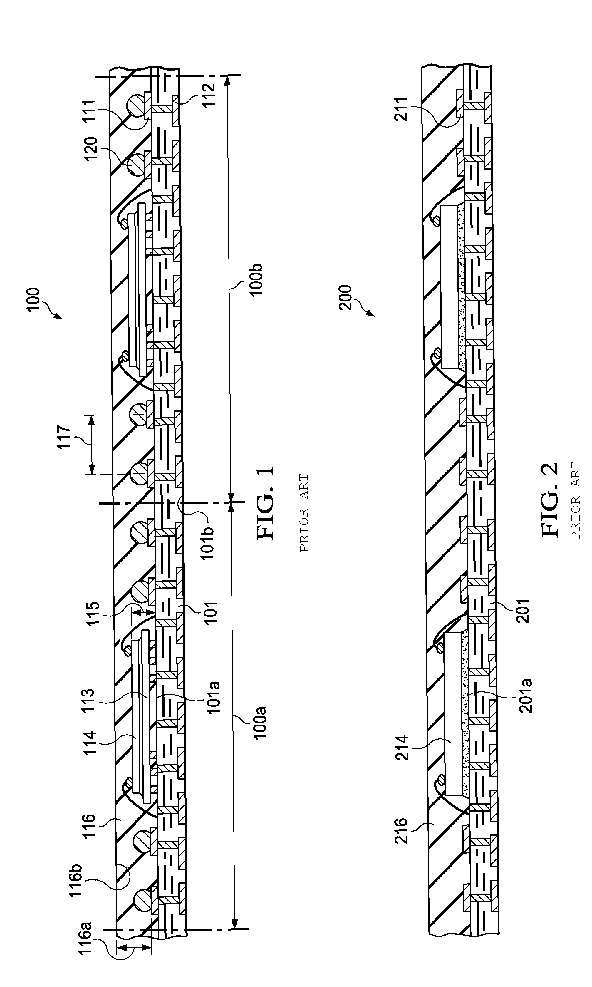
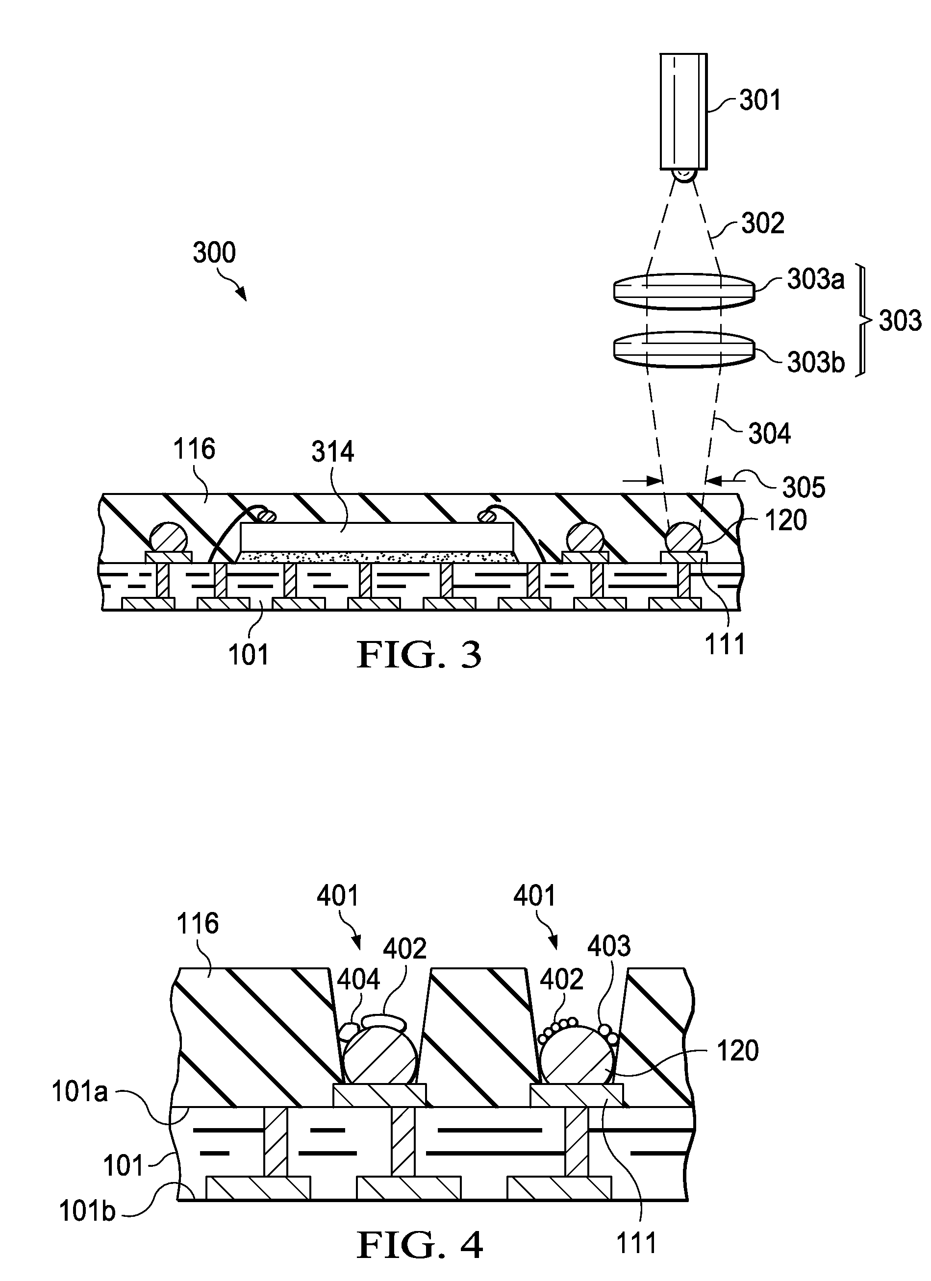
[0018]FIGS. 1 to 3 depict exemplary semiconductor products at certain stages of their fabrication process to illustrate embodiments of the invention. FIGS. 4 to 6 show steps and results of the cleaning method. Referring now to FIG. 1, the semiconductor device generally designated 100 includes a strip of substrate 101 made of an insulating material yet integral with conductive lines and vias. Substrate 101 has a first side 101a and a second side 101b. On first side 101a are first contact pads 111, and on second side 101b are second contact pads 112. First and second contact pads are preferably made of copper or aluminum. Substrate 101 includes a plurality of sites 100a, 100b, etc. for assembling semiconductor chips and fabricating units of semiconductor devices.

[0019]The area of each substrate site 100a, 100b, etc. is divided into a region, preferably in the approximate center of the of the site area, which is reserved for assembling semiconductor chips. Dependent on the device type ...


PUM

PropertyMeasurementUnit
heightaaaaaaaaaa
thicknessaaaaaaaaaa
thicknessaaaaaaaaaa

Abstract

A process flow exposing and cleaning contact surfaces employing a liquid cleaning agent such as flux to penetrate the interface between the glassy coats and the surface of metal and to delaminate the coats from the metal, and then, at elevated temperatures, to use the agent's vapor pressure to break up the glassy coats into smaller pieces. The glassy coats are prevented by their low density to penetrate into the molten solder. Finally, at ambient temperature, the floating filler debris is water-washed and rinsed away. Cleaning agents include low-viscosity liquids (oils) and flux, which do not decompose at elevated temperatures and are mixed with components operable to provide, at the elevated temperatures, the fumes for sufficient vapor pressure to break up and dislodge the coats from the metal contacts.

Description

FIELD OF THE INVENTION[0001]The present invention is related in general to the field of semiconductor devices and processes and more specifically to the fabrication method of solder connections to metal contacts of a device, which is covered by an insulating layer so that windows have to be opened to expose the contacts.DESCRIPTION OF RELATED ART[0002]It has been common practice for several decades to connect semiconductor devices to external parts such as printed circuit boards by soldering. The solder may be provided by a paste, a previously deposited solder amount, or by a solder ball. The solder connection technology has recently been extended to an emerging product family called package-on-package (PoP) devices, wherein a top device package is aligned with a bottom device package, and the output terminals of the top package are connected with the input terminals of the bottom package. Commonly, the connection of terminals is achieved by reflowing the solder body attached to eac...

Claims


Application Information

Patent Timeline
Patent Type & Authority Patents(United States)
IPC IPC(8): B08B7/00
CPCH01L23/3128H01L24/97H01L25/50H01L24/16H01L24/32H01L24/48H01L25/0657H01L25/105H01L2224/16225H01L2224/32145H01L2224/32225H01L2224/48091H01L2224/48227H01L2224/48465H01L2224/73265H01L2224/97H01L2225/0651H01L2225/06517H01L2225/06558H01L2924/01013H01L2924/01029H01L2924/01047H01L2924/01079H01L2924/01082H01L2924/15331H01L2924/1815H01L2224/81H01L2224/85H01L2924/00014H01L2924/01006H01L2924/01033H01L2924/01074H01L2924/01075H01L2924/01322H01L2924/014H01L2924/00H01L2924/00012H01L2924/181H01L24/73H01L2924/14H01L2224/45099H01L2224/45015H01L2924/207
Inventor GERBER, MARK AWACHTLER, KURT P
Owner TEXAS INSTR INC
Why Eureka
Try Eureka