
Omnidirectional Eddy Current Array Probes and Methods of Use

a technology of eddy current array and probe, which is applied in the direction of magnetic property measurement, material magnetic variables, instruments, etc., can solve the problems of low detectability, frequent inspection of surface flaws of aircraft components formed of conductive materials, and cracks in different orientations

Inactive Publication Date: 2010-04-08
GENERAL ELECTRIC CO
View PDF16 Cites 6 Cited by
  • Summary
  • Abstract
  • Description
  • Claims
  • Application Information

AI Technical Summary

Benefits of technology

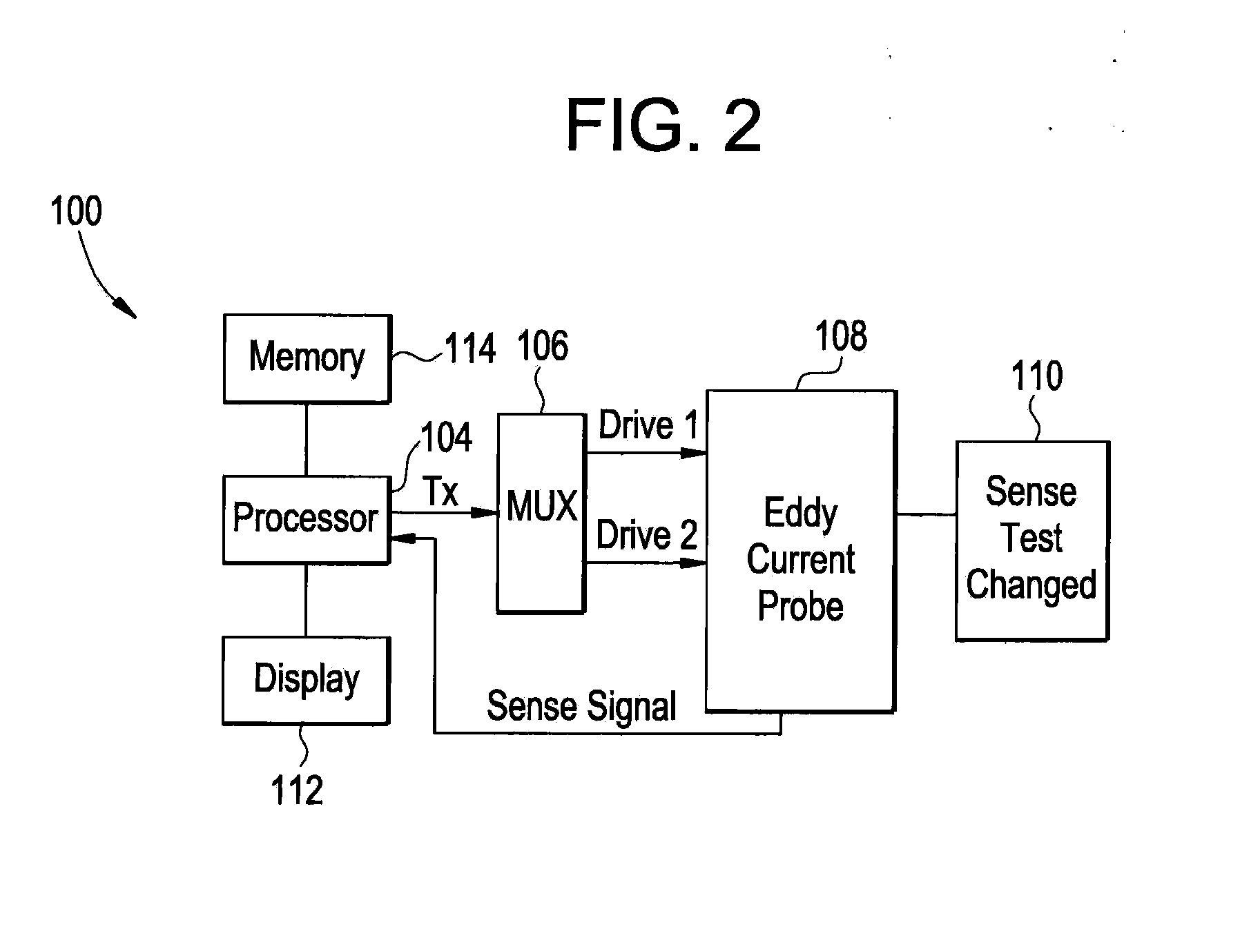
The present invention provides an omnidirectional eddy current array probe for detecting flaws at different orientations in a conductive test object. The probe includes a first row of drive lines and at least one additional row, which are superimposed over each other to induce eddy currents in the test object. The sensing portion operates to sense the eddy currents and output a signal indicative of the sensed eddy currents. The technical effect of this invention is that it allows for more accurate and efficient detection of flaws in conductive test objects.

Problems solved by technology

For example, aircraft components formed of conductive materials often need to be inspected for surface flaws such as cracks.
However, in several situations such as, for example, the flat area of an engine disk, cracks can occur in different orientations.
However, current eddy current array probes usually are made up of discrete elements and typically have regions through which small flaws can pass through with low detectability.
However, flaws parallel to the array length that are close to the size of the gap between elements can pass through with low sensitivity.
Compensation of the responses from this probe is oftentimes difficult due to the complicated footprints.
Another problem is that the high number of drive vias can result in low fabrication yields.

Method used


Image

  • Omnidirectional Eddy Current Array Probes and Methods of Use
  • Omnidirectional Eddy Current Array Probes and Methods of Use
  • Omnidirectional Eddy Current Array Probes and Methods of Use

Examples


Embodiment Construction

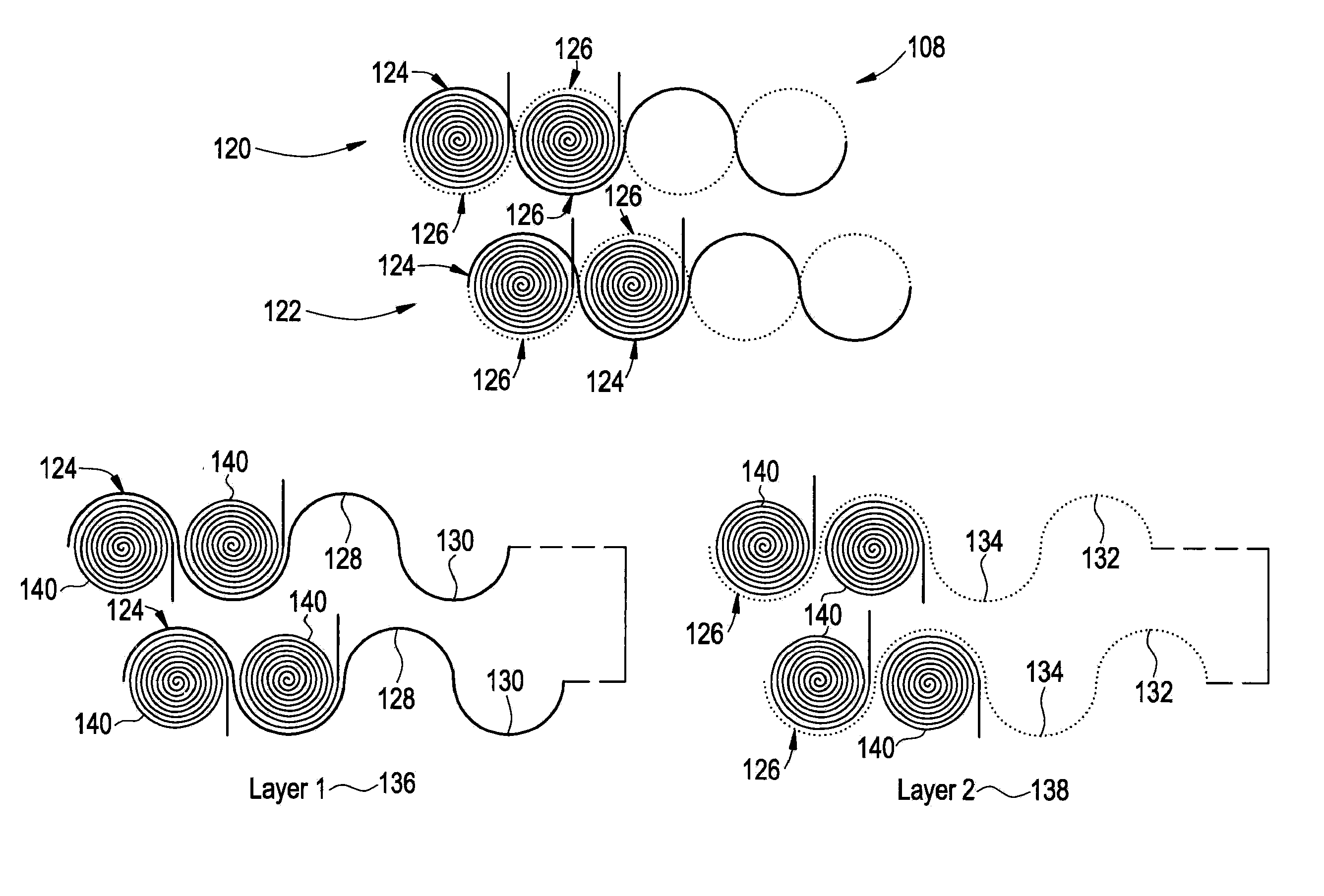
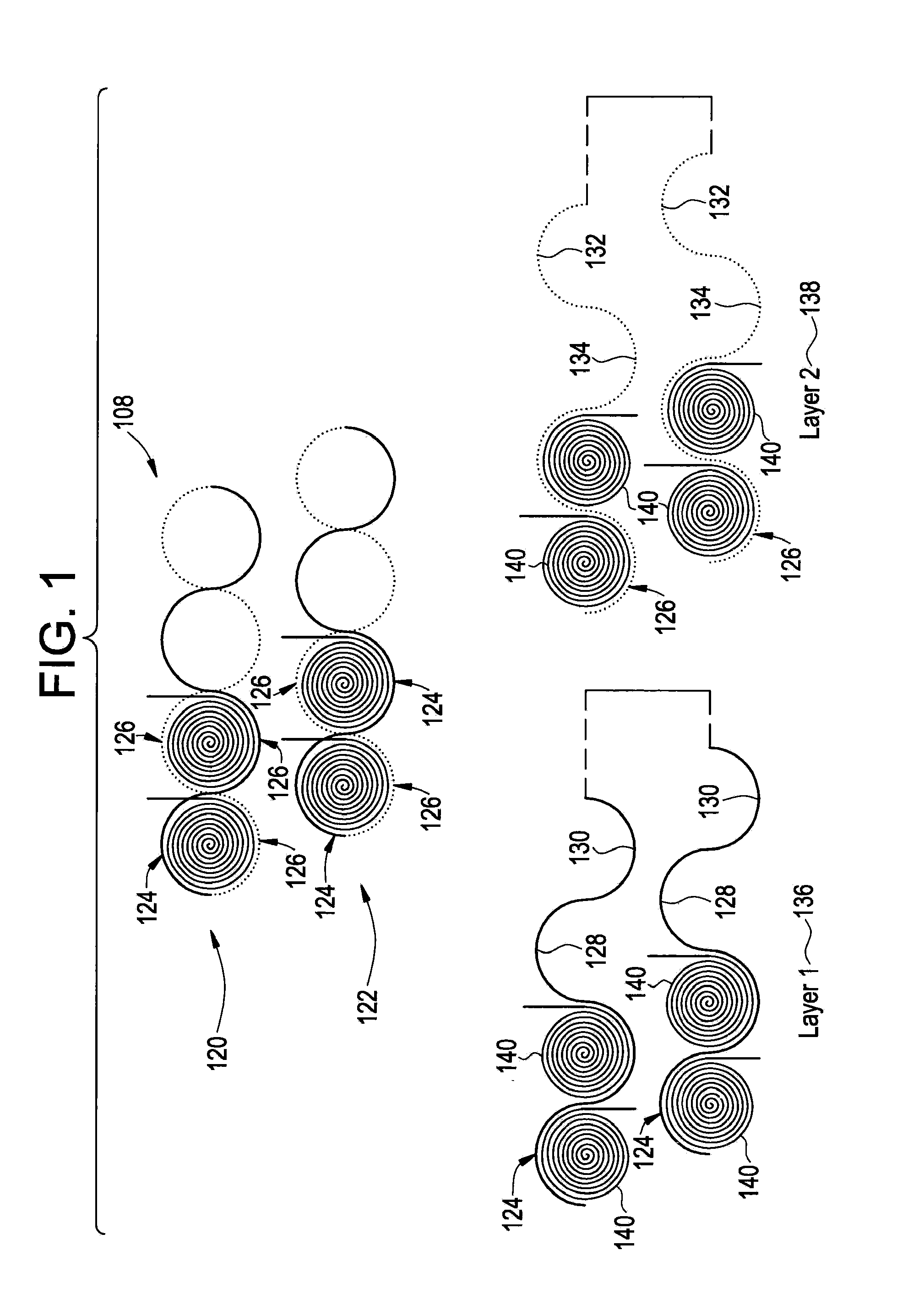
[0017]Disclosed herein are omnidirectional eddy current array probes and non-destructive methods for detecting flaws in / on conductive objects and / or substrates. Unlike the prior art, the omnidirectional eddy current array probes disclosed herein use complementary and symmetrical drive lines disposed in two or more rows and layers in a continuous manner to detect flaws at different orientations without blind zones (i.e., less sensitive zones). Although circular symmetry is shown and generally discussed herein, other shapes are contemplated, e.g., square, oval, rectangular, and the like. In one embodiment, the omnidirectional eddy current array probe employs four semi-circular wave shaped continuous drive lines in two or more rows disposed in two or more layers that are multiplexed for omnidirectional inspection without blind spots. In one embodiment, each row is offset laterally from an adjacent row by a distance equal to a quarter wavelength of the wave pattern so as to provide omni...


PUM

PropertyMeasurementUnit
eddy current arrayaaaaaaaaaa
conductiveaaaaaaaaaa
eddy currentaaaaaaaaaa

Abstract

Omnidirectional eddy current array probes for detecting flaws in a conductive test object generally includes semi-circular wave shaped continuous drive lines in two rows disposed in two layers that are multiplexed for omnidirectional inspection without blind spots. The semicircular wave shaped continuous drive lines are superimposed to form pseudo-circular drive lines, wherein each row of drive lines is offset laterally by a distance preferably equal to a quarter wavelength of the wave pattern. For only parallel and perpendicular flaws, the drive multiplexing is not needed and each row will have only one set of drive lines. In alternate embodiments, there can be square-shaped, oval shaped, rectangular-shaped or other shaped wave patterns as well. Also disclosed are methods for sensing surface flaws and compensating their response.

Description

BACKGROUND[0001]This disclosure generally relates to probes and methods for non-destructive evaluation, and more specifically, to eddy current probes and methods for non-destructive inspection of conductive test objects.[0002]Industrial processes often use non-destructive examination to test and / or inspect an object without damaging the object. For example, aircraft components formed of conductive materials often need to be inspected for surface flaws such as cracks. One such method for non-destructive testing of conductive materials for flaws is eddy current inspection. Eddy current inspection is accomplished with probes configured to have current flow in a drive coil line, which results in an electromagnetic field being created. The electromagnetic field induces eddy currents on the metallic test object. The eddy currents so induced in turn generate a secondary magnetic field, which creates a potential difference in sensors (coils or other transducers), whose outputs may be analyz...

Claims


Application Information

Patent Timeline
Patent Type & Authority Applications(United States)
IPC IPC(8): G01N27/90
CPCG01N27/9033G01N27/9006
Inventor SHEILA-VADDE, APARNA CHAKRAPANISUH, UI WONWANG, CHANGTING
Owner GENERAL ELECTRIC CO
Learn More