Optical Ovonic Threshold Switch

a threshold switch and optical ovonic technology, applied in the field of electronic switching, can solve the problems of blockage of signal transmission between interconnected circuit elements and destruction of conductive pathways, and achieve the effect of high conductivity

Active Publication Date: 2010-05-13
OVONYX MEMORY TECH LLC
View PDF8 Cites 4 Cited by
  • Summary
  • Abstract
  • Description
  • Claims
  • Application Information

AI Technical Summary

Benefits of technology

This patent describes how to use chalcogenide materials to make switches by getting them excited without using any electricity. An external magnetic force causes the material to change from being insulating to becoming highly conductive through the action of certain particles called lone pairs. By adjusting the strength of the magnet, researchers have been able to control the size of these conductive paths and achieve very low resistance at high levels of activity.

Problems solved by technology

The technical problem addressed in this patent text is how to improve the performance of computers and make them faster and more efficient compared to traditional silicon-based technologies. There is a limit to what achievements can be made using standard techniques like reducing the dimension of semiconductor devices. To overcome this limitation, researchers have explored alternative computing mechanisms, such as chalcogenide phase change materials. However, existing solutions require significant investments in advanced fabrication methods and face issues with scaling down to extremely small levels of organization. Therefore, the goal is to extend the range of devices and functional activities available from chalcogenide materials and allow for greater speed operation.

Method used


Image

  • Optical Ovonic Threshold Switch
  • Optical Ovonic Threshold Switch

Examples


Embodiment Construction

[0015]Although this invention will be described in terms of certain preferred embodiments, other embodiments that are apparent to those of ordinary skill in the art, including embodiments that do not provide all of the benefits and features set forth herein, are also within the scope of this invention. Accordingly, the scope of the invention is defined only by reference to the appended claims.

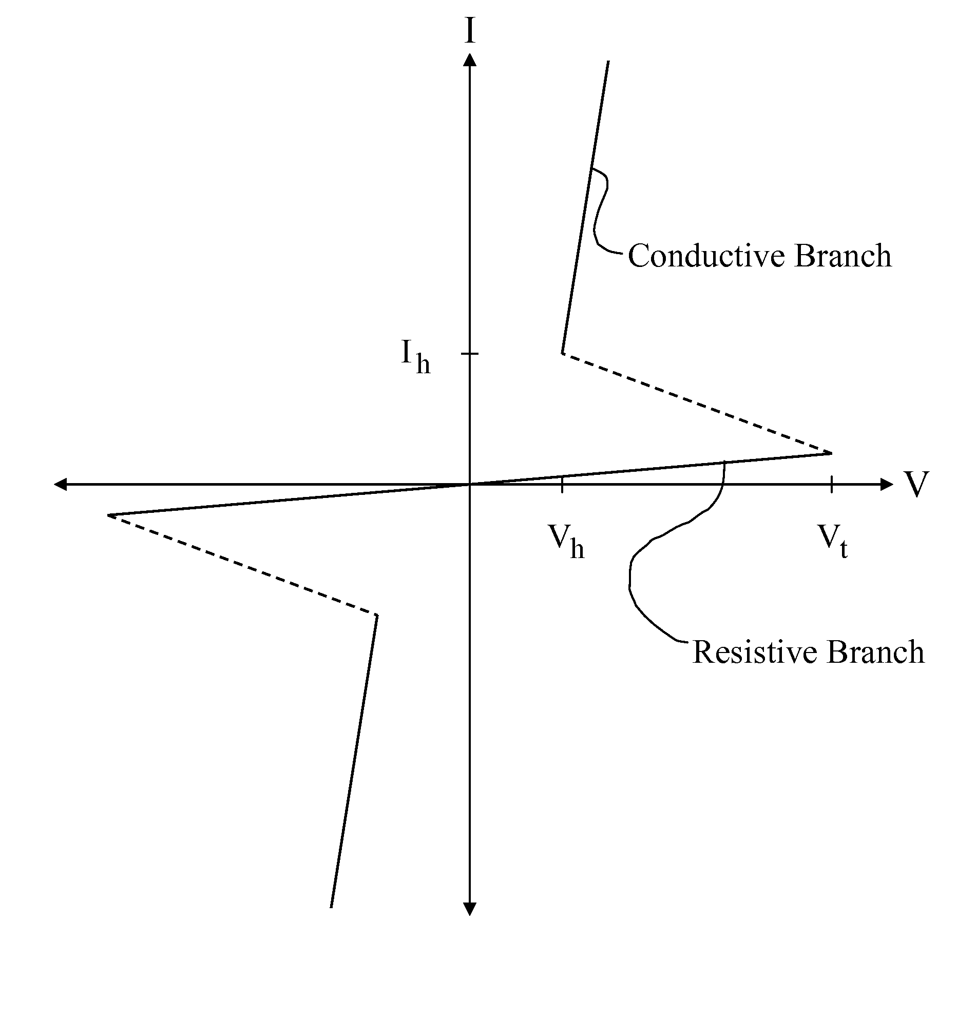
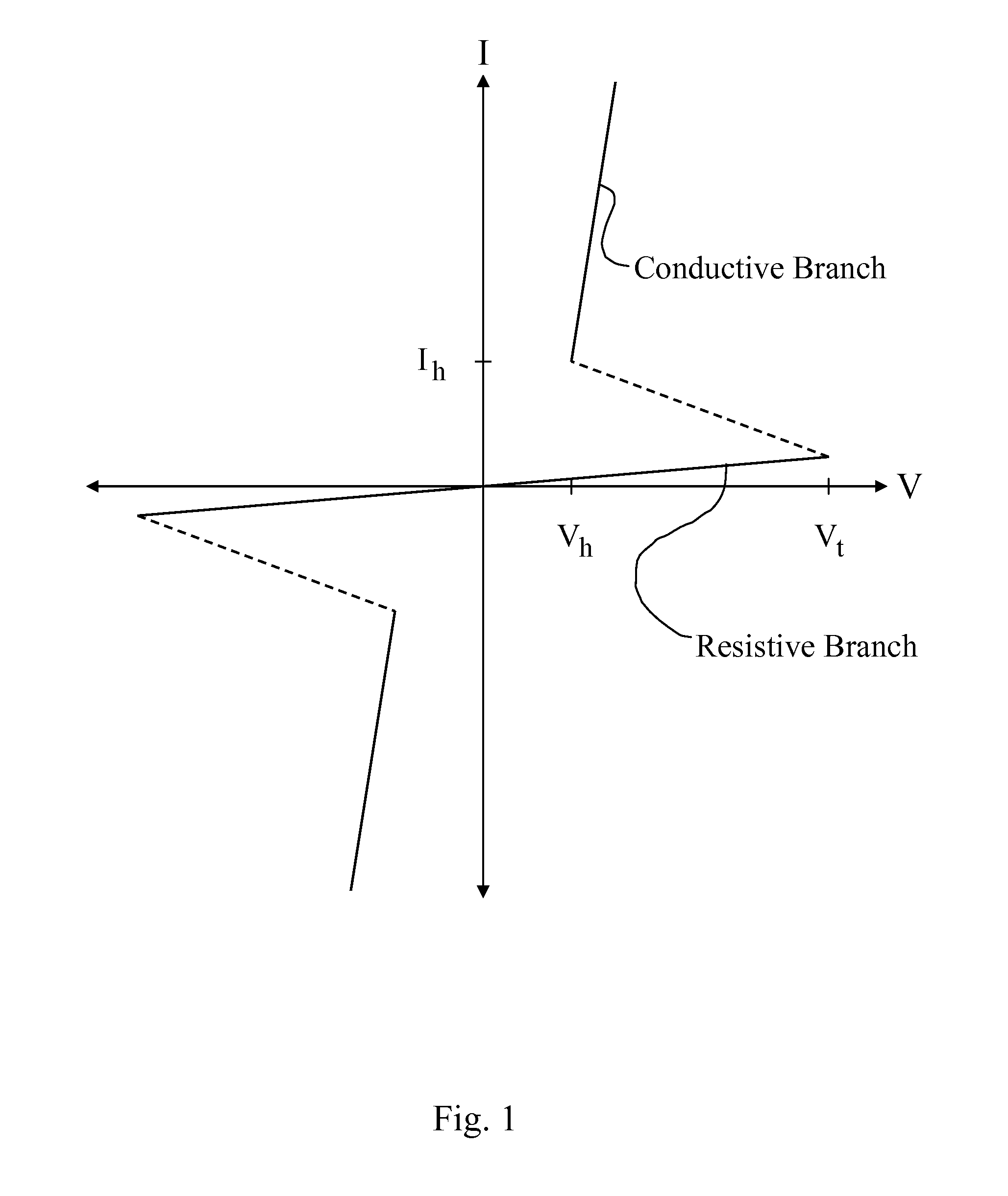
[0016]The instant invention provides a method and device for initiating a transformation of an active material from an electrically resistive state to an electrically conductive state using a non-electrical source of energy. The active material may be referred to herein as a switching material. Among the important switching materials are the chalcogenide switching materials, also known as Ovonic threshold switching or OTS materials. The electrically-induced switching characteristics of OTS materials have been described in U.S. Pat. Nos. 5,543,737; 5,694,146; and 5,757,446; the disclosures of wh...


PUM


Abstract

A method and device for accomplishing transformation of a switching material from a resistive state to a conductive state. The method utilizes a non-electrical source of energy to effect the switching transformation. The switching material may be a chalcogenide switching material, where the non-electrical source of energy initiates switching by liberating lone pair electrons from bound states of chalcogen atoms. The liberated lone pair electrons form a conductive filament having the characteristics of a solid state plasma to permit high current densities to pass through the switching material. The device includes a switching material with electrical contacts and may be interconnected with other elements in a circuit to regulate electrical communication therebetween.

Description


Claims


Application Information

Patent Timeline
Owner OVONYX MEMORY TECH LLC
Why Eureka
Try Eureka