
Display, display panel, method for inspecting display panel and method for manufacturing display panel

a technology for display panels and display devices, applied in the direction of discharge tubes luminescent screens, instruments, lighting and heating apparatus, etc., can solve the problems of large time requirements for recognizing and the inability to completely sort out defective organic electroluminescent device products

Inactive Publication Date: 2010-06-10
PIONEER CORP
View PDF9 Cites 2 Cited by
  • Summary
  • Abstract
  • Description
  • Claims
  • Application Information

AI Technical Summary

Benefits of technology

The invention is a display device comprising an organic electroluminescent device with a transparent electrode and an emission sealing layer that emits light by an electric field generated between the electrodes. The device includes a driving circuit that provides an applied voltage to the electrodes to drive each organic electroluminescent device of the display panel. The invention also includes a method for inspecting defects in the emission sealing layer and a method for manufacturing the display panel. The technical effects of the invention include improved display quality and efficiency, reduced power consumption, and improved manufacturing process control.

Problems solved by technology

At this time, however, a non-luminous region of the organic electroluminescent device referred to as a “dark spot” may increase in size, resulting in a defect.
The main cause of such a dark spot is a pinhole that occurs during film formation.
Nevertheless, in a case where a point defect that cannot be completely covered by a buffer layer exists, a great amount of time is generally required to recognize the spot as a large non-luminous defect of the display device prior to product shipment.
Thus, in the inspection stage performed prior to shipment, the problem arises that defective organic electroluminescent device products cannot be completely sorted out.

Method used


Image

  • Display, display panel, method for inspecting display panel and method for manufacturing display panel
  • Display, display panel, method for inspecting display panel and method for manufacturing display panel
  • Display, display panel, method for inspecting display panel and method for manufacturing display panel

Examples


embodiment 1

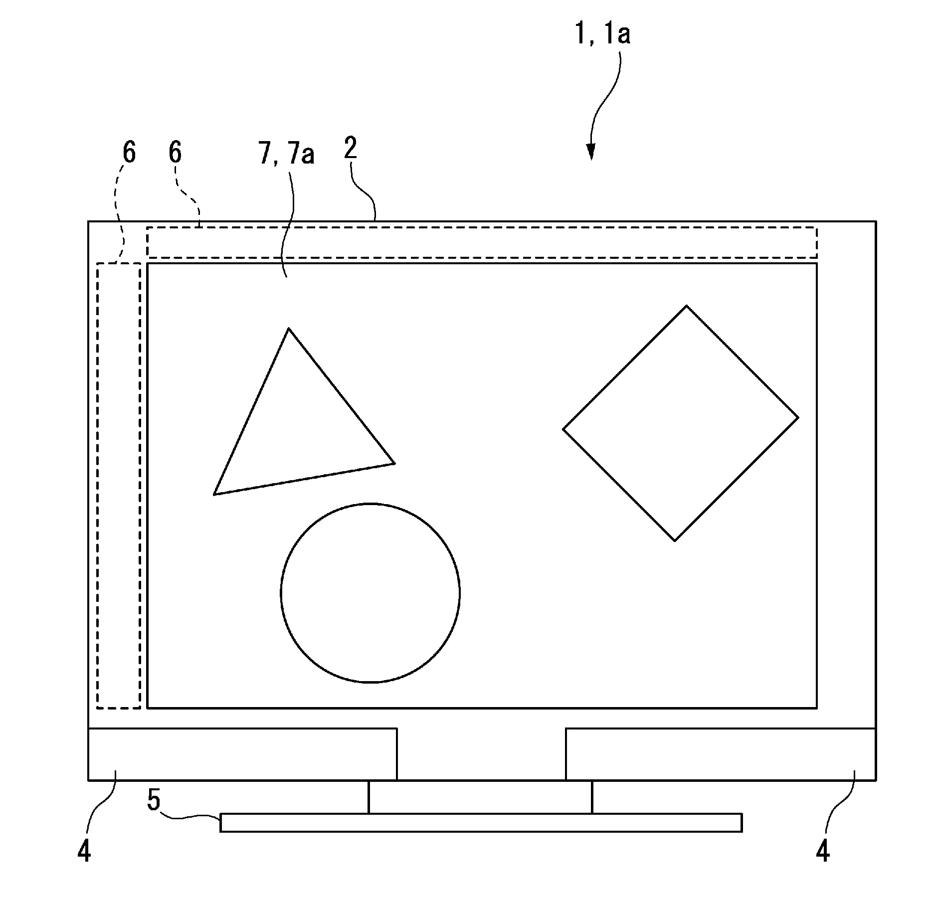
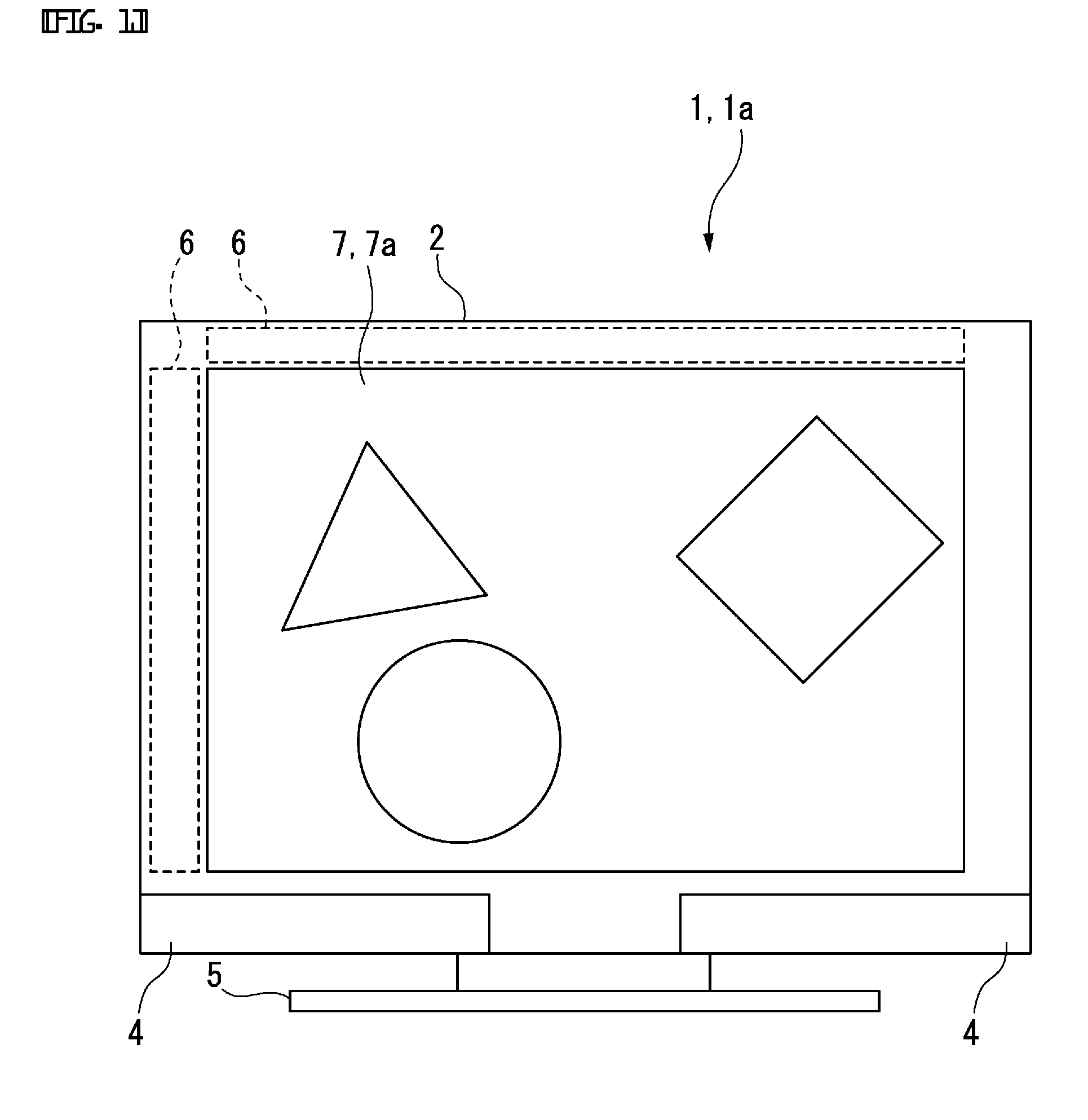
[0029]FIG. 1 is a front view illustrating an example of the outer appearance of a display device 1 comprising an organic electroluminescent device 3 of embodiment 1.

[0030]The display device 1 has a housing 2 and legs 5. The housing 2 is supported on an installation surface by the legs 5. This housing 2 visually comprises a display panel 7 and two speakers 4. The display panel 7 is provided at the center of the housing 2 and, at this center of the housing 2, has a function of displaying images based on image data inputted from an external source. The speakers 4 are respectively provided on the right side and left side underneath the housing 2.

[0031]The speakers 4 have a function of outputting sound in synchronization with the image displayed on the display panel 7. The housing 2 comprises a drive circuit 6 within its interior. This drive circuit 6 performs drive control for displaying images based on the aforementioned image data on the display panel 7.

[0032]The display panel 7 is a ...

embodiment 2

[0076]FIG. 9 is a cross-sectional view illustrating a configuration example of an organic electroluminescent device 3a built into a display device 1a of embodiment 2.

[0077]This organic electroluminescent device 3a involves substantially the same configuration, substantially the same operation, and substantially the same manufacturing method as those of embodiment 1. The same reference numerals as the numerals in FIG. 1 to FIG. 8 will therefore be employed for identical components, identical operations, and identical manufacturing methods and descriptions thereof will be omitted. The following description will focus on the unique points of this embodiment.

[0078]In the organic electroluminescent device 3a of embodiment 2, unlike embodiment 1, the emission sealing layer 8 comprises a multi-layered configuration rather than a single-layered configuration as described above. Specifically, in embodiment 2, as illustrated in FIG. 9, a separate emission sealing layer 11 is formed so as to c...


PUM


Abstract

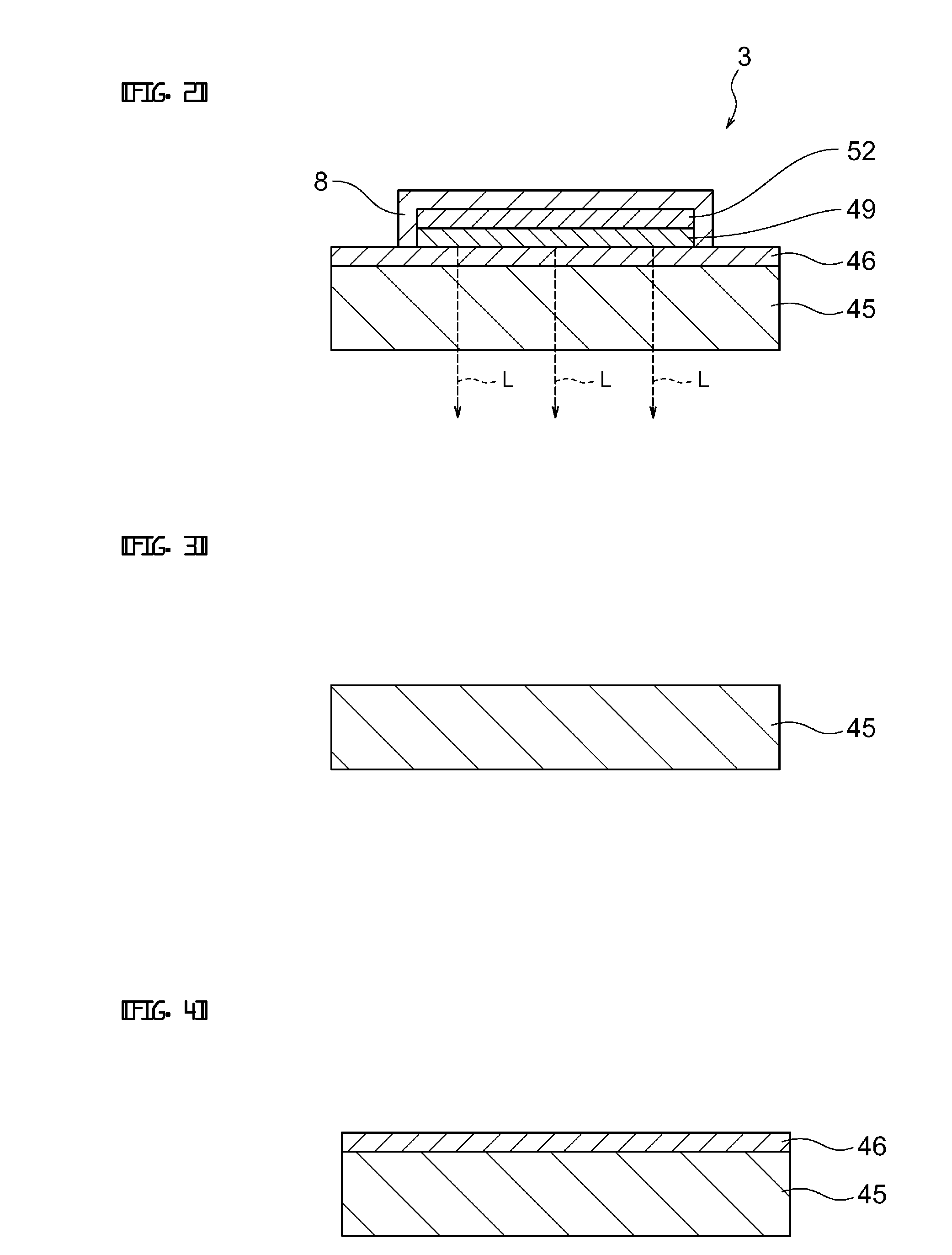
An organic electroluminescent device comprising a plurality of electrodes stacked on a substrate, at least one of the electrodes being transparent, an organic electroluminescent layer that is layered between the plurality of electrodes and emits light by an electric field generated between the plurality of electrodes by an applied voltage, and emission sealing layers that are members that seal the plurality of electrodes and the organic electroluminescent layer and emit light by light excitation, is provided.

Description

CROSS-REFERENCE TO RELATED APPLICATION[0001]This is an application PCT / JP2007 / 56646, filed Mar. 28, 2007, which was not published under PCT article 21(2) in English.BACKGROUND OF THE INVENTION[0002]1. Field of the Invention[0003]The present invention relates to a display device, display panel, display panel inspection method, and display panel manufacturing method comprising an organic electroluminescent device wherein an organic electroluminescent layer emits light by an electric field generated in a plurality of electrodes.[0004]2. Description of the Related Art[0005]In recent years, display devices that employ a so-called organic electroluminescent device have been developed as the next generation display to replace the liquid crystal display. A display that employs such an electroluminescent device (hereinafter “organic EL display”) is capable of achieving high-brightness light emission even at a low voltage.[0006]Such an organic EL display has attracted much attention as a self...

Claims


Application Information

Patent Timeline
Patent Type & Authority Applications(United States)
IPC IPC(8): G09G5/00H01J1/62H01J9/42H01J9/26
CPCH01L27/322H05B33/10H05B33/04H01L51/5237H10K59/38H10K59/873H10K50/844
Inventor SHIRATORI, MASAHIRO
Owner PIONEER CORP
Learn More