ESD detection circuit and related method thereof

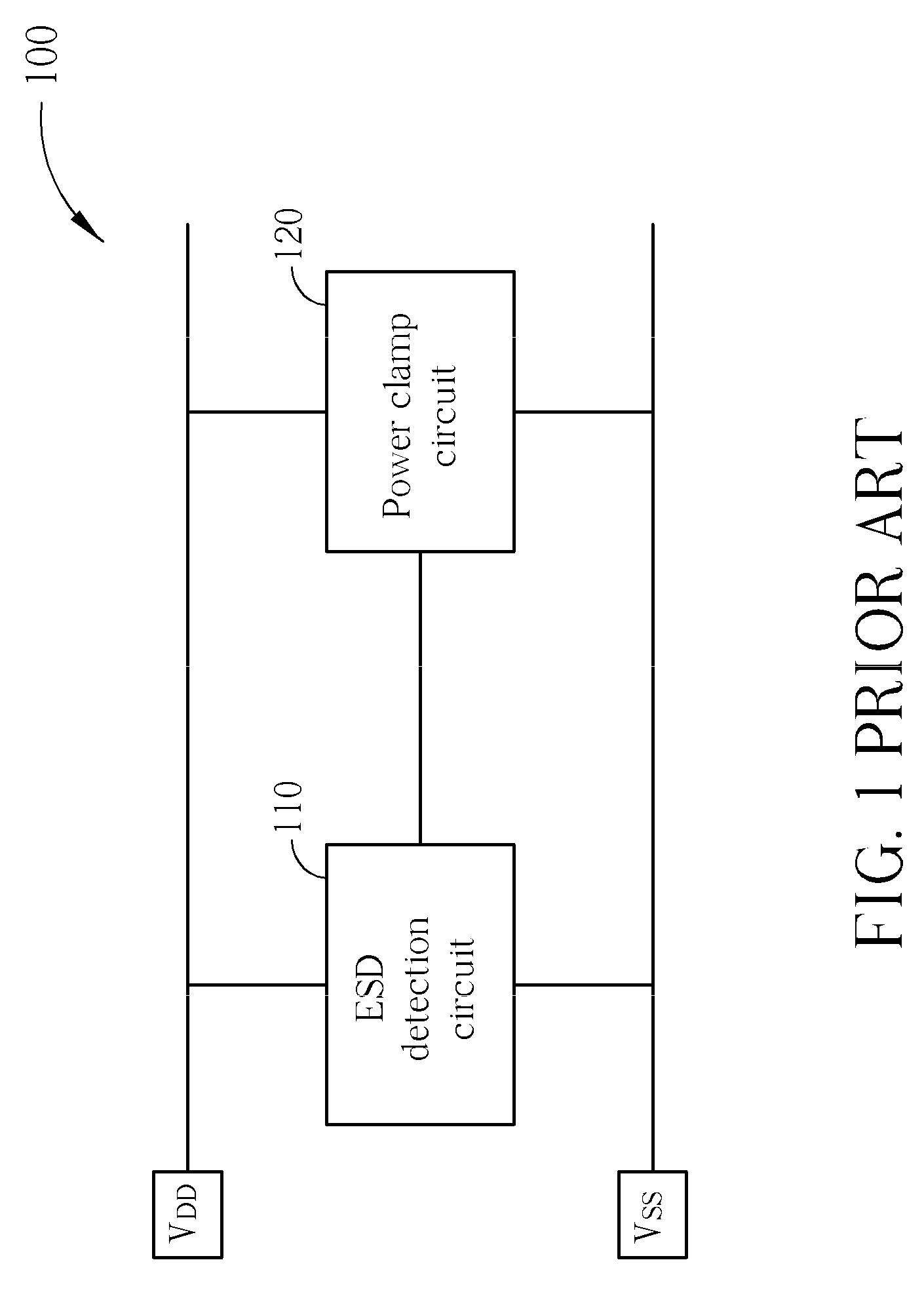
a detection circuit and detection method technology, applied in the direction of air-break switches, emergency protective arrangements for limiting excess voltage/current, semiconductor/solid-state device details, etc., can solve the problems of external static electricity easily damaging the inner circuit of the chip to be damaged or interfered, and the damage or interference of the chip

Active Publication Date: 2010-06-17
FARADAY TECH CORP
View PDF3 Cites 28 Cited by
  • Summary
  • Abstract
  • Description
  • Claims
  • Application Information

AI Technical Summary

Benefits of technology

[0014]It is therefore an objective of the present invention to solve the aforementioned problems, and to provide ESD circuits with various circuit structures and methods thereof to eliminate the unwanted leakage current of the ESD detection circuit that occurs by virtue of using electronic components complying with a modern nano scale process. In addition, the ESD detection circuit disclosed in the present invention is coupled to a ground terminal indirectly via a bias circuit rather than directly coupled to the ground terminal. By applying the bias circuit, the present ESD protection circuit has a smaller voltage difference between two terminals of a MOS capacitor in a resistor-capacitor circuit and hence eliminates the excessive unwanted leakage current in the modern electronic circuits complying with an advanced nano scale process.
[0017]By the disclosed ESD detection circuit and method thereof the leakage current of ESD detection circuit when no ESD events occur is eliminated and this therefore solves the problem for modern ESD detection circuit(s) of the ESD protection circuit applying electronic transistors having a thinner gate oxide thickness.

Problems solved by technology

However, during processes such as packaging, testing, delivering, and manufacturing, etc, the chip can be damaged or interfered with by the external static electricity via the electronic pads (power pads and signal pads) of the chip.
External static electricity easily damages inner circuits in a chip via the electronic pads, and the unwanted condition causing the inner circuits of a chip to be damaged or interfered with is called electrostatic discharge (ESD).
Providing excellent ESD protection circuits for protecting modern integrated electronic circuits (e.g., a chip) from being damaged by the unwanted ESD noise is an important issue for designers.
However, a gate oxide thickness of a MOS capacitor complying with the advanced nano scale process is thinner than that of a MOS capacitor complying with a conventional process and this thereby leads to the ESD detection circuit with excessive leakage current.
The unwanted excessive leakage current probably makes the ESD protection circuit 200 to operate in error.
For instance, a malfunction of the ESD protection circuit occurs due to the leakage current to thereby induce the ESD protection circuit to output the ESD trigger signal Itrigger incorrectly and result in even more serious leakage current.
The PMOS transistor 221 hence turns on and makes the ESD trigger signal Itrigger convert from a low logic level into a high logic level in error, resulting in the following ESD protection components (e.g., clamp circuit) to operate erroneously.

Method used


Image

  • ESD detection circuit and related method thereof
  • ESD detection circuit and related method thereof
  • ESD detection circuit and related method thereof

Examples


Embodiment Construction

[0027]Certain term are used throughout the following description and claims to refer to particular system components. As one skilled in the art will appreciate, manufacturers may refer to a component by different names. This document does not intend to distinguish between components that differ in name but not function. In the following discussion and in the claims, the terms “including” and “comprising” are used in an open-ended fashion, and thus should be interpreted to mean “including, but not limited to . . . .” The terms “couple” and “couples” are intended to mean either an indirect or a direct electrical connection. Thus, if a first device couples to a second device, that connection may be through a direct electrical connection, or through an indirect electrical connection via other devices and connections.

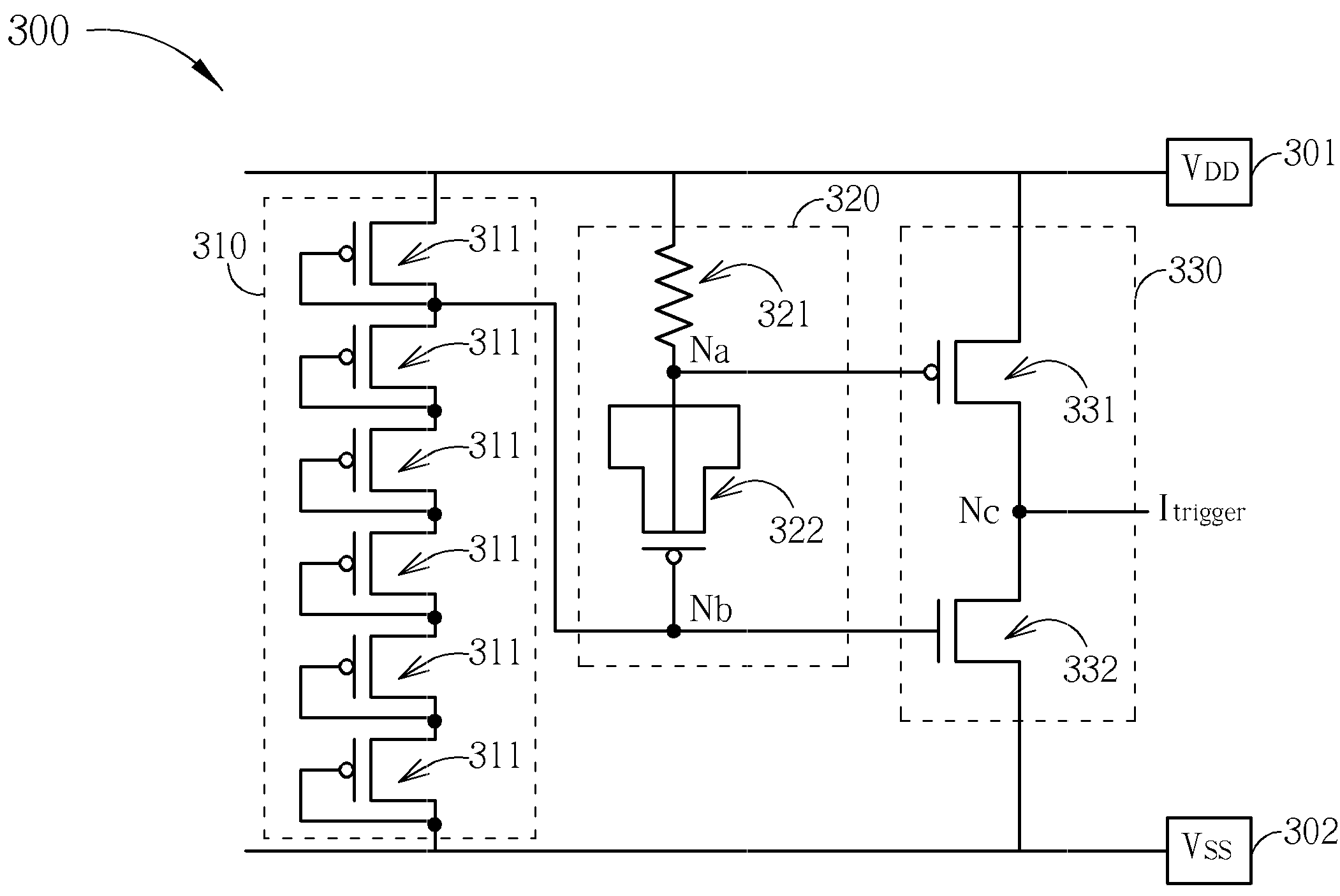
[0028]Please refer to FIG. 3. FIG. 3 is a diagram illustrating an electro-static discharge (ESD) detection circuit according to a first exemplary embodiment of the present i...


PUM


Abstract

An electro-static discharge (ESD) detection circuit is provided. The ESD detection circuit includes: a first power pad for receiving a first supply voltage; a second power pad for receiving a second supply voltage; an RC circuit having an impedance component coupled between the first power pad and a first terminal and having an capacitive component coupled between the first terminal and a second terminal, wherein the second terminal is not directly connected to the second supply voltage; a trigger circuit couples to the first power pad, the second power pad, and the RC circuit, for generating an ESD trigger signal according to a voltage level at the first terminal and a voltage level at the second terminal, and a bias circuit coupled between the first power pad and the second power pad for providing a bias voltage to the second terminal.

Description

BACKGROUND OF THE INVENTION[0001]1. Field of the Invention[0002]The present invention relates to ESD protection, and more particularly, to an ESD detection method and related method thereof for ESD protecting circuits applying electronic elements complying with a nano scale process.[0003]2. Description of the Prior Art[0004]The development of semiconductor processes is ongoing. As one skilled in the art will appreciate, a modern chip is allowed to have a plurality of various electronic circuits configured within. Moreover, electronic pads are disposed on each chip for receiving an external power source (e.g., a bias current / voltage) and for exchanging data with other external electronic circuits / chips. For instance, a chip has power pads implemented for receiving bias voltage(s), and signal pads for receiving input signals and output signals. The above-mentioned signal pads are named I / O pads.[0005]That is, the chip is connected with external electronic circuits or chips via the afo...

Claims


Application Information

Patent Timeline
Patent Type & Authority Applications(United States)
IPC IPC(8): H01H31/02H02H7/00
CPCH02H9/046
Inventor KER, MING-DOUCHIU, PO-YENHUANG, CHUN
Owner FARADAY TECH CORP
Why Eureka
Try Eureka