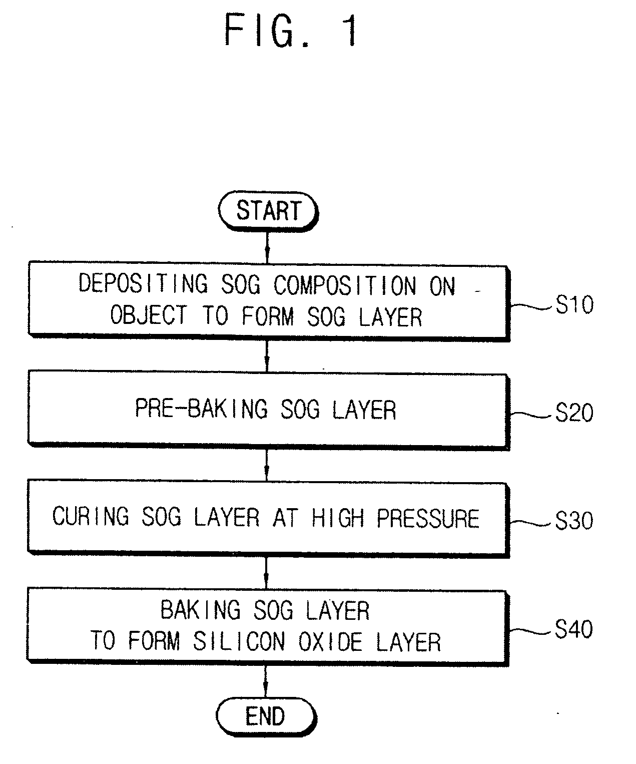
Methods of forming a silicon oxide layer and methods of forming an isolation layer
a technology of silicon oxide layer and isolation layer, which is applied in the direction of coatings, electrical appliances, basic electric elements, etc., can solve the problems of generating cracks or voids in the resultant silicon oxide layer, affecting the stability of the substrate, so as to prevent (or reduce the likelihood of) damage to the substrate. , the effect of rapid shrinkage of the sog layer
- Summary
- Abstract
- Description
- Claims
- Application Information
AI Technical Summary
Benefits of technology
Problems solved by technology
Method used
Image

Examples
example 1
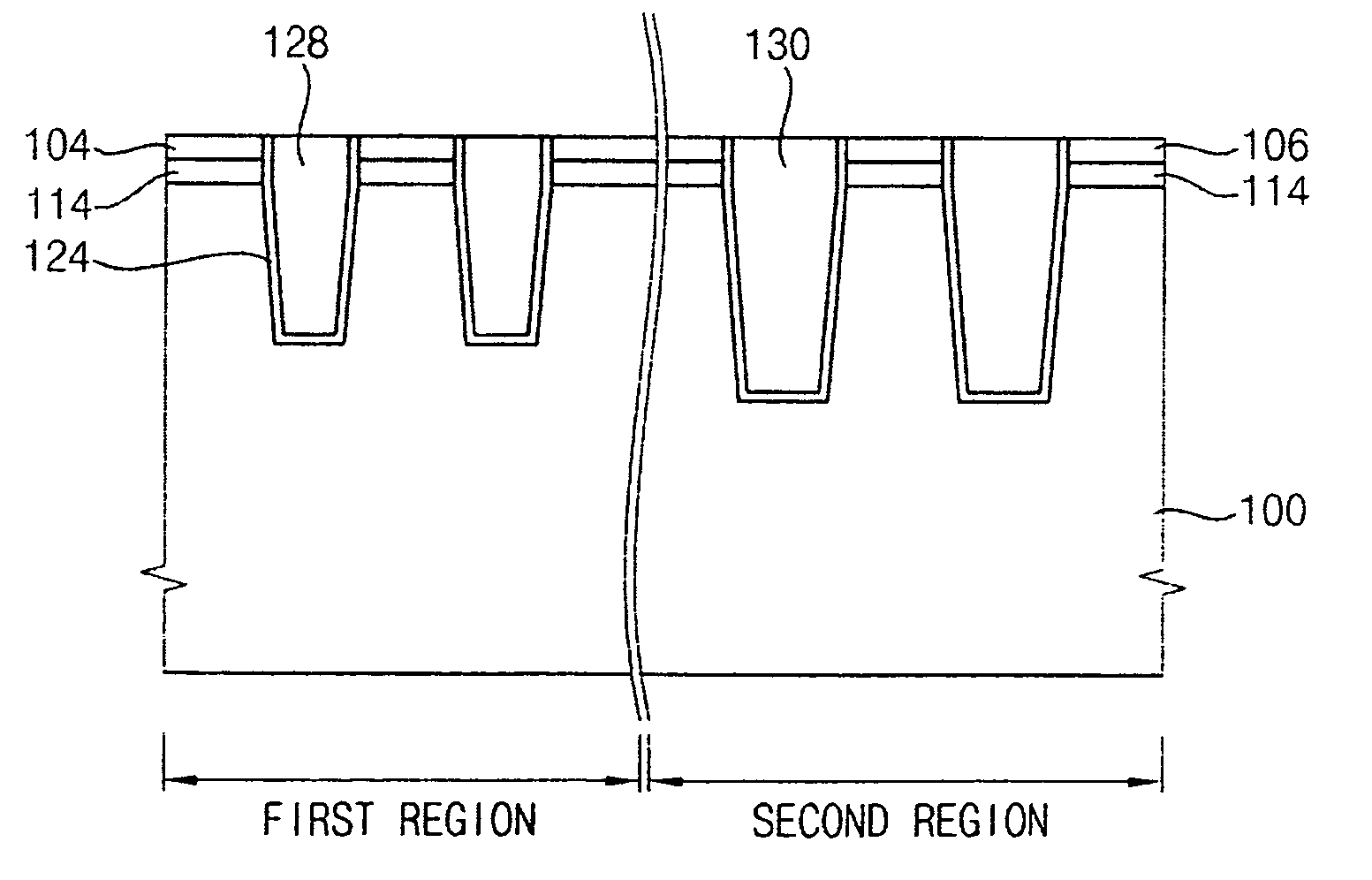
[0138]First patterns spaced apart from each other by about 500 Å were provided in a first region of a substrate, and second patterns spaced apart from each other by about 1,000 Å were provided in a second region of a substrate. The substrate was etched using the first patterns and the second patterns as etching masks to form a first trench having a depth of about 2,000 Å in the first region and a second trench having a depth of about 5,000 Å in the second region of the substrate. An SOG layer burying the first and second trenches was formed on the substrate using an SOG composition including about 20% by weight of perhydropolysilazane.
[0139]A first pre-baking process at about 120° C. and a second pre-baking process at about 300° C. were performed on the SOG layer. A curing process was performed on the substrate including the pre-baked SOG layer. The curing process was performed after disposing the substrate in an autoclave of which pressure was set to about 2 atm and of which temper...
example 2
[0141]A silicon oxide layer pattern burying a first trench and a second trench on a substrate was formed by performing substantially the same procedure described in Example 1 except that the curing process was performed by setting the temperature of the autoclave to about 105° C. and contacting the pre-baked SOG layer with deionized water instead of ozone. The difference in distance (nm), along the x-axis and y-axis of the substrate, between the position of the silicon oxide layer patterns burying the first and second trenches and the position of the first and second patterns on the substrate was measured. Mean values of the measured values are illustrated in FIG. 13.
example 3
[0142]A silicon oxide layer pattern burying a first trench and a second trench on a substrate was formed by performing substantially the same procedure described in Example 1 except that the curing process was performed by setting the temperature of the autoclave to about 105° C. The difference in distance (nm), along the x-axis and y-axis of the substrate, between the position of the silicon oxide layer patterns burying the first and second trenches and the position of the first and second patterns on the substrate was measured. Mean values of the measured values are illustrated in FIG. 13.
PUM
| Property | Measurement | Unit |
|---|---|---|
| Temperature | aaaaa | aaaaa |
| Temperature | aaaaa | aaaaa |
| Temperature | aaaaa | aaaaa |
Abstract
Description
Claims
Application Information
 - R&D Engineer
- R&D Manager
- IP Professional
- Industry Leading Data Capabilities
- Powerful AI technology
- Patent DNA Extraction
Browse by: Latest US Patents, China's latest patents, Technical Efficacy Thesaurus, Application Domain, Technology Topic.
© 2024 PatSnap. All rights reserved.Legal|Privacy policy|Modern Slavery Act Transparency Statement|Sitemap