Electrode Structure, Device Comprising the Same and Method for Forming Electrode Structure

a technology of electrode structure and electrode, which is applied in the direction of solid-state devices, basic electric elements, semiconductor devices, etc., can solve the problems of annihilating holes, and reducing the efficiency associated with generating current or carriers, so as to prevent hole annihilation and imperfection formation, the effect of increasing the generation efficiency of carriers

Inactive Publication Date: 2010-07-22
VEECO ALD
View PDF100 Cites 44 Cited by
  • Summary
  • Abstract
  • Description
  • Claims
  • Application Information

AI Technical Summary

Benefits of technology

[0013]Embodiments provide an electrode structure, device and method for increasing carrier generation efficiency by preventing hole annihilation and formation of imperfection in a thin film.

Problems solved by technology

Thee annihilation of the holes tends to lower the efficiency associated with generating current or carriers (e.g., electrons or holes) by exposing the solar cell or the display device to the sunlight.
Furthermore, a thin film obtained by CVD or PVD may have degraded physical, chemical and electrical properties due to defects, impurities, defects of crystalline structure, imperfect grain boundary, or the like.
The degraded properties is detrimental to generation and diffusion of carrier due to the sunlight, and results in poor performance associated with drift and the like.
As a result, the thin-film type solar cells generally tend to exhibit lower short circuit current and lower efficiency compared to the bulk type solar cell and are more susceptible to light induced aging.

Method used


Image

  • Electrode Structure, Device Comprising the Same and Method for Forming Electrode Structure
  • Electrode Structure, Device Comprising the Same and Method for Forming Electrode Structure
  • Electrode Structure, Device Comprising the Same and Method for Forming Electrode Structure

Examples


Embodiment Construction

[0029]Hereinafter, exemplary embodiments of the present invention will be described in detail with reference to the accompanying drawings. However, the present invention is not limited the following exemplary embodiments.

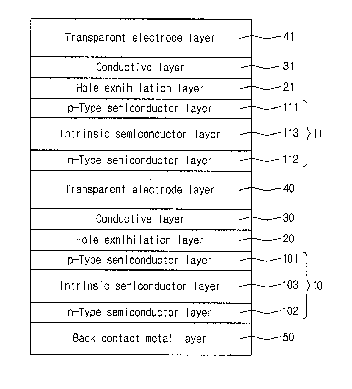
[0030]FIG. 2 is a schematic sectional view of an electrode structure according to an exemplary embodiment. The electrode structure of FIG. 2 includes a semiconductor junction 10, a hole exnihilation layer 20 and a transparent electrode layer 40. The semiconductor junction 10 may include a p-type semiconductor layer 101 and an n-type semiconductor layer 102. For example, the semiconductor junction 10 may be a p-n junction in which one p-type semiconductor layer 101 is joined with one n-type semiconductor layer 102. Alternatively, the semiconductor junction 10 may be a p-i-n junction in which an intrinsic semiconductor layer (not shown) is further interposed between the p-type and n-type semiconductor layers 101 and 102. As a further alternative embodiment, the semico...


PUM


Abstract

An electrode structure comprises a semiconductor junction comprising an n-type semiconductor layer and a p-type semiconductor layer; a hole exnihilation layer on the p-type semiconductor layer; and a transparent electrode layer on the hole exnihilation layer. The electrode structure further comprises a conductive layer between the hole exnihilation layer and the transparent electrode layer. In the electrode structure, one or more of the hole exnihilation layer, the conductive layer and the transparent electrode layer may be formed by an atomic layer deposition. In the electrode structure, a transparent electrode formed of a degenerated n-type oxide semiconductor does not come in direct contact with a p-type semiconductor, and thus, annihilation or recombination of holes generated in the p-type semiconductor can be reduced, which increases the carrier generation efficiency. Further, the electric conductivity of the transparent electrode is increased by the conductive layer, which improves electrical characteristics of a device.

Description

CROSS-REFERENCE TO RELATED APPLICATION[0001]This application claims priority from and the benefit under 35 U.S.C. §119(e) of U.S. patent application No. 61 / 146,161, filed on Jan. 21, 2009, which is incorporated by reference herein in its entirety.BACKGROUND[0002]1. Field of the Invention[0003]Embodiments relate to an electrode structure for a solar cell having a transparent electrode.[0004]2. Description of the Related Art[0005]Some thin-film type solar cells include a transparent electrode, a p-n junction and a metal film. The transparent electrode is generally made of a transparent material that allows sunlight to pass through and has excellent electric conductivity characteristics. The p-n junction is formed of a p-type semiconductor material and an n-type semiconductor material. The p-n junction may be in the form of a p-i-n junction that includes an undoped layer of intrinsic semiconductor material sandwiched between a layer of p-type semiconductor material and a layer of n-typ...

Claims


Application Information

Patent Timeline
Patent Type & Authority Applications(United States)
IPC IPC(8): H01L29/22H01L29/861H01L21/36H01L31/0296H01L31/18
CPCH01L21/02554H01L21/02565H01L21/02576H01L21/02579Y02E10/50H01L31/022466H01L31/075H01L31/078H01L31/1884H01L21/0262H01L31/022475H01L31/022483Y02E10/548
Inventor LEE, SANG IN
Owner VEECO ALD
Why Eureka
Try Eureka