Solid-state imaging device

a solid-state imaging and imaging device technology, applied in the direction of radioation control devices, television system scanning details, television systems, etc., can solve the problems of limiting the readout operation to 2, difficult to achieve the dynamic range improvement of output signals, and, more broadly, the image quality of the solid-state imaging device that performs the conventional two-way operation

Inactive Publication Date: 2010-07-22
PANASONIC CORP
View PDF9 Cites 2 Cited by
  • Summary
  • Abstract
  • Description
  • Claims
  • Application Information

AI Technical Summary

Benefits of technology

[0009]While the above conventional solid-state imaging device improves a trade-off between the image quality and the output time by the two-way transfer, its readout operation is limited to 2:1 interlace (see FIGS. 2A and 2B of Japanese Patent No. 3,277,974). That is, it is impossible to divide a frame into multiple fields utilizing multiple-to-one interlace for the readout and transfer of the signal charges.
[0010]The multiple-to-one interlace is a technique for increasing a saturation signal charge amount of the vertical charge-coupled devices to improve a dynamic range of an output signal, and is frequently used in solid-state imaging devices using a single horizontal charge-coupled device.

Problems solved by technology

While the above conventional solid-state imaging device improves a trade-off between the image quality and the output time by the two-way transfer, its readout operation is limited to 2:1 interlace (see FIGS. 2A and 2B of Japanese Patent No. 3,277,974).
That is, it is impossible to divide a frame into multiple fields utilizing multiple-to-one interlace for the readout and transfer of the signal charges.
Because of an inability to adopt this technique, it is difficult to achieve improvement in dynamic range of the output signal and, more broadly, in image quality in the solid-state imaging device that performs the conventional two-way transfer.

Method used


Image

  • Solid-state imaging device
  • Solid-state imaging device
  • Solid-state imaging device

Examples


Embodiment Construction

[0038]Hereinafter, a CCD imaging device according to one embodiment of the present invention will be described in detail with reference to the accompanying drawings.

[0039]

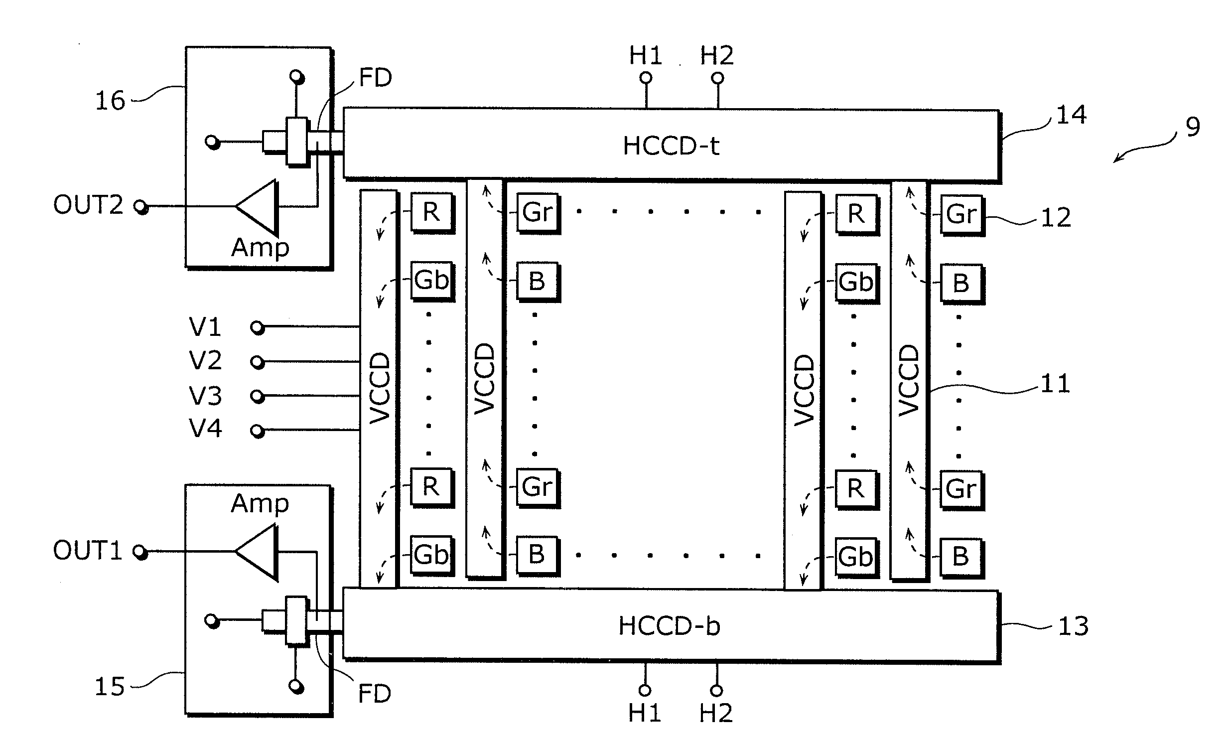
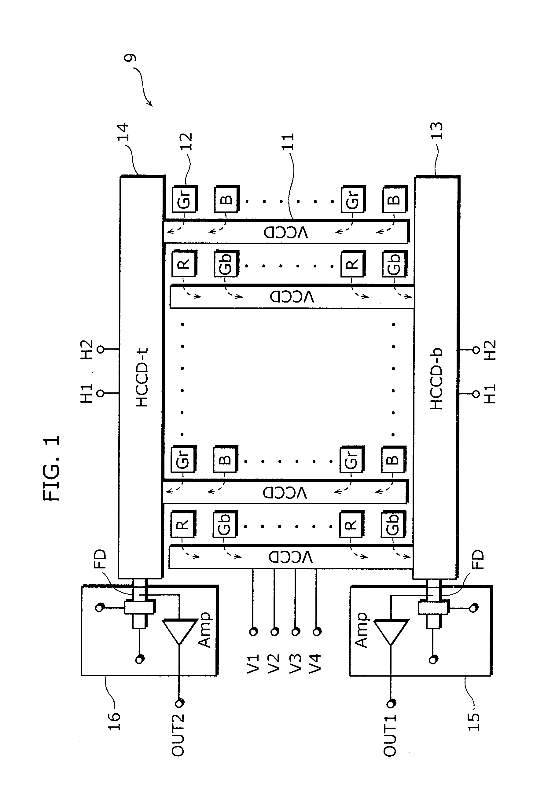
[0040]FIG. 3 is a block diagram illustrating an exemplary functional structure of a CCD imaging device 1 according to one embodiment of the present invention.

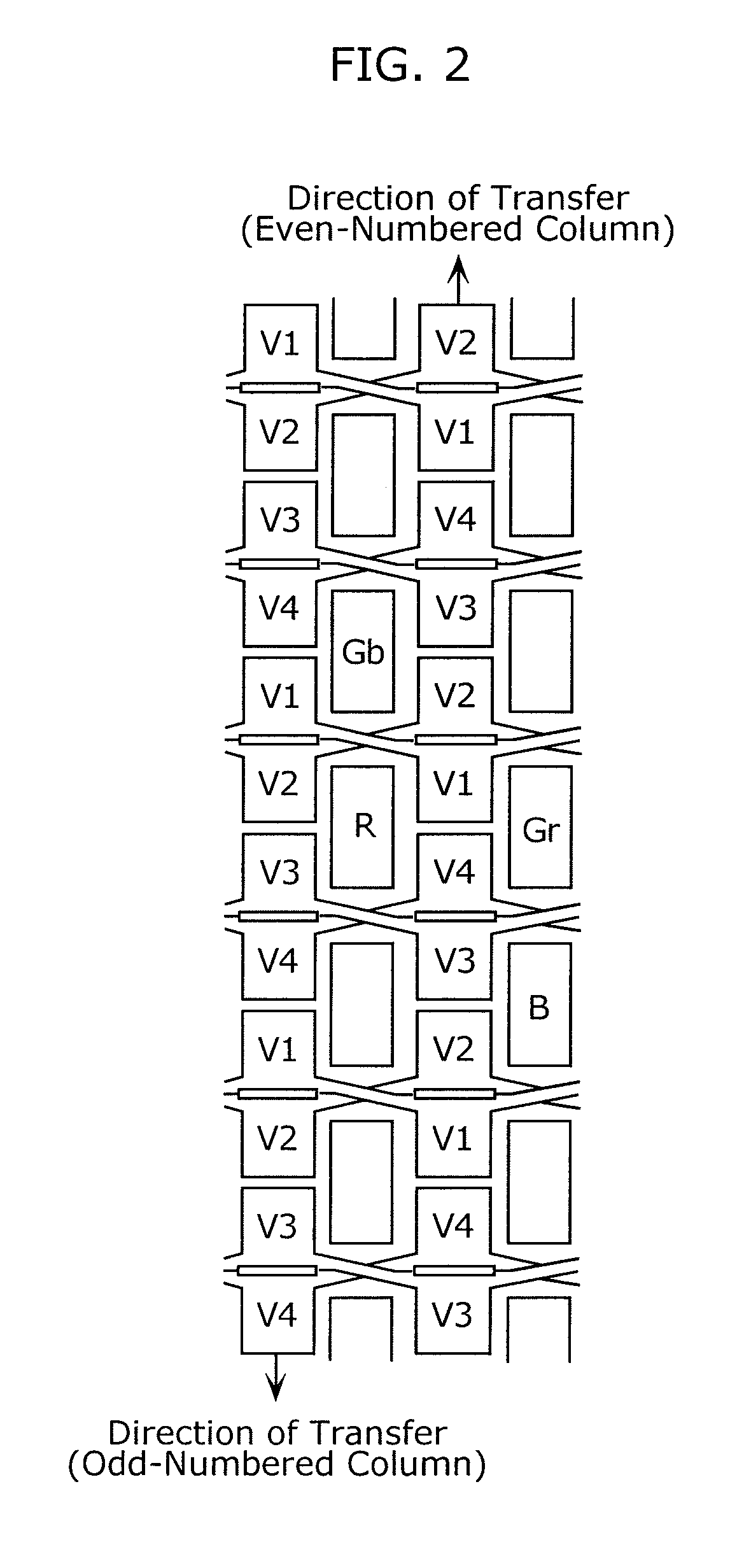
[0041]The CCD imaging device 1 includes an imaging area having vertical CCDs 11, which are represented by vertically oriented rectangles labeled “VCCD”, and photodiodes 12, which are represented by squares labeled “R”, “Gr”, “Gb”, or “B”. In the imaging area, odd-numbed (counting from the left) vertical CCDs transfer signal charges from the photodiodes in a downward direction, whereas even-numbered vertical CCDs transfer the signal charges from the photodiodes in an upward direction.

[0042]A horizontal CCD 13 and a horizontal CCD 14 are arranged below and above the imaging area, respectively. Signals outputted from left ends of the horizontal CCDs 13 and 14 are...


PUM


Abstract

In a solid-state imaging device, photodiodes (12) are classified into a plurality of fields, and each one of driving pulses (V1A, V1B, V2, V3A, V3B, V4) is applied to corresponding one of the photodiodes via a plurality of electrodes (17). Of the electrodes, a plurality of electrodes used to control readout of the signal charges from the photodiodes to the charge-coupled devices (11) are interconnected such that each one of a plurality of independent driving pulses (V1A, V1B, V3A, V3B) is applied to the corresponding one of the electrodes in accordance with the number of fields into which the photodiodes are classified.

Description

TECHNICAL FIELD[0001]The present invention relates to a solid-state imaging device in which signal charges are read out using charge-coupled devices, and a method of driving the same.BACKGROUND ART[0002]Solid-state imaging devices are widely used in which a plurality of signal charges obtained from a plurality of photodiodes arranged cyclically on a two-dimensional plane are transferred using vertical charge-coupled devices (VCCDs) each of which is placed in a separate column, and thereafter the signal charges are transferred using a horizontal charge-coupled device (HCCD: Horizontal CCD) to be outputted to the outside. Such solid-state imaging devices are also called CCD imaging devices.[0003]FIG. 1 is a block diagram illustrating an exemplary structure of a conventional CCD imaging device 9 disclosed in Japanese Patent No. 3,277,974.[0004]FIG. 2 is a diagram illustrating arrangement of control signal lines that are used to apply driving pulses V1 to V4 to VCCDs 11 in the CCD imagi...

Claims


Application Information

Patent Timeline
Patent Type & Authority Applications(United States)
IPC IPC(8): H04N5/335H01L27/148H04N5/341H04N5/357H04N5/369H04N5/372
CPCH01L27/14812H01L27/14837H04N5/3456H04N9/045H04N5/37213H04N5/3728H04N5/3452H04N5/3595H04N25/441H04N25/445H04N25/625H04N25/713H04N25/73
Inventor YONEMOTO, KAZUYA
Owner PANASONIC CORP
Why Eureka
Try Eureka