Liquid crystal display device and method of manufacturing same

a technology of liquid crystal display and liquid crystal, which is applied in non-linear optics, instruments, optics, etc., can solve the problems of reducing display quality and yield in production, and achieve the effect of high display quality and less visible defects in the illumination poin

Inactive Publication Date: 2010-07-22
SHARP KK
View PDF11 Cites 62 Cited by
  • Summary
  • Abstract
  • Description
  • Claims
  • Application Information

AI Technical Summary

Benefits of technology

[0034]The present invention makes luminance point defects less noticeable and therefore provides a liquid crystal display device having high display quality.

Problems solved by technology

The luminance point defect greatly reduce the display quality and yield in production.

Method used


Image

  • Liquid crystal display device and method of manufacturing same
  • Liquid crystal display device and method of manufacturing same
  • Liquid crystal display device and method of manufacturing same

Examples


Embodiment Construction

[0052]An embodiment of the present invention will be explained with reference to FIGS. 1 to 10.

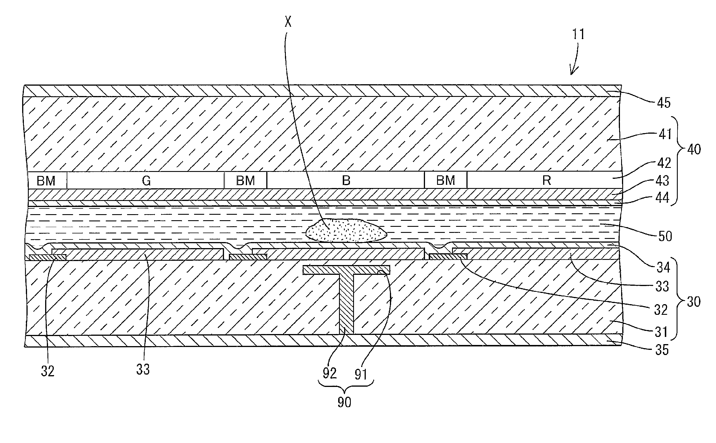
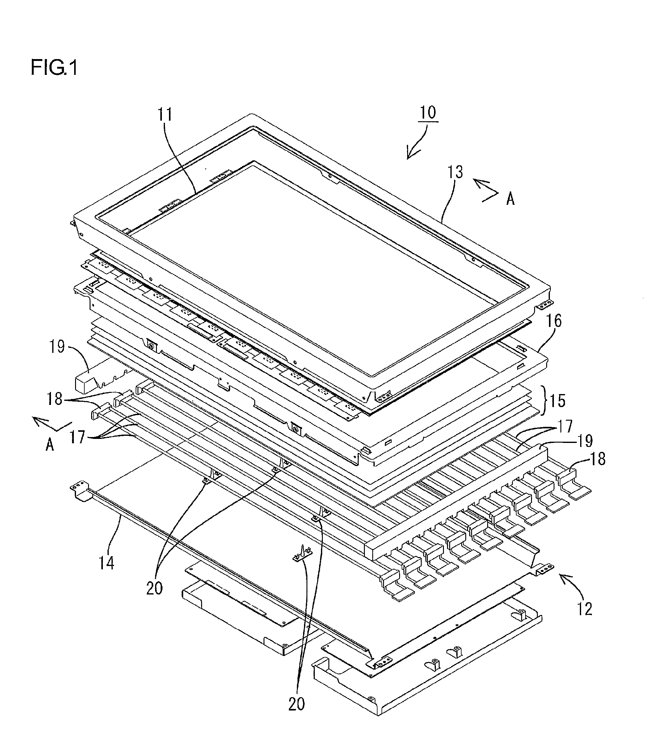
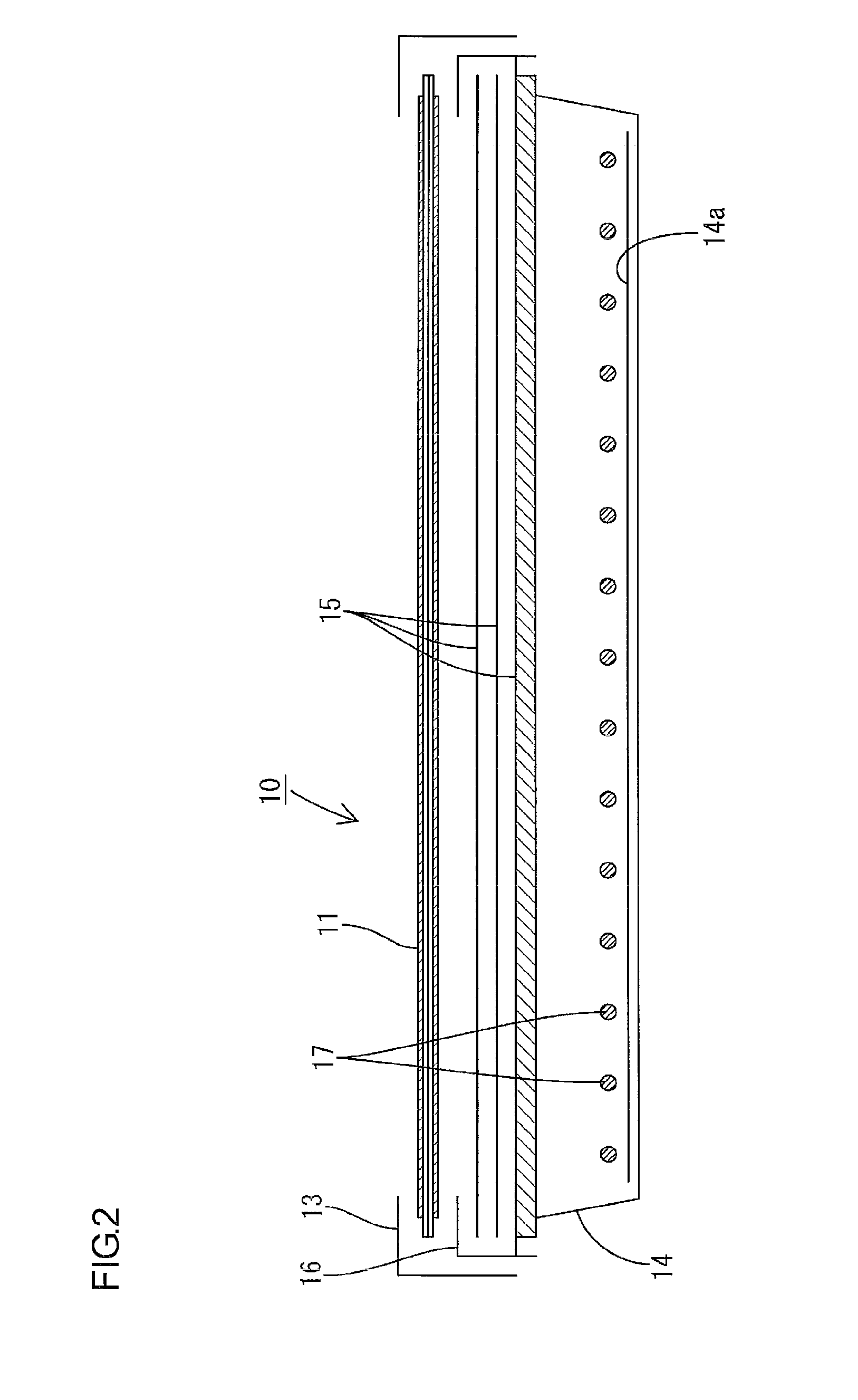
[0053]FIG. 1 is a perspective view illustrating a general construction of a liquid crystal display device according to an embodiment of the present invention. FIG. 2 is a cross-sectional view of the liquid crystal display device illustrated in FIG. 1 along the line A-A. FIG. 3 is a vertical sectional view of a main part of a liquid crystal panel included in the liquid crystal display device illustrated in FIG. 1. FIG. 4 is a horizontal sectional view of a main part of the liquid crystal panel. FIG. 5 is an explanatory view explaining operational effect of the liquid crystal display device of the embodiment. FIG. 6 is an explanatory view explaining an illumination inspection process for a liquid crystal panel, which is an inspection object. FIG. 7 is a side view illustrating a general construction of a luminance point defect compensation device. FIGS. 8 to 10 are explanatory views explainin...


PUM

PropertyMeasurementUnit
wavelengthaaaaaaaaaa
luminanceaaaaaaaaaa

Abstract

A liquid crystal display device 10 of the present invention includes a liquid crystal panel 11 and a lighting device 12. The liquid crystal panel 11 has a liquid crystal layer 50 between a pair of glass substrates 31 and 41. The lighting device 12 provides illumination light to the liquid crystal panel 11. An externally communicable void section 63 is formed in the glass substrate 31 among the pair of glass substrates 31 and 41 in an area that can block light toward a luminance point defect occurrence area X, which is a possible cause of a luminance point defect. The externally communicable void section 63 has a void portion 61 that is formed in the glass substrate 31 and a through portion that penetrates from the void portion 61 through an opposite surface of the glass substrate 31 from the liquid crystal layer 50. A light blocking layer 60 is formed in the externally communicable void section 63.

Description

TECHNICAL FIELD[0001]The present invention relates to a liquid crystal display device and a method of manufacturing the liquid crystal display device.BACKGROUND ART[0002]The following is an example of method of manufacturing a liquid crystal display device. Switching elements (e.g., TFT) and pixel electrodes are disposed on one of glass substrates provided in a pair, and counter electrodes are arranged on the other glass substrate. Those glass substrates are then bonded with spacers between them. Liquid crystal is injected between the glass substrates so as to form a liquid crystal layer. Then, polarizing plates are attached to respective surfaces of the glass substrates to produce a liquid crystal panel. A lighting device that has a plurality of cold cathode tubes as light source is provided for the liquid crystal panel.[0003]Such a manufacturing process of liquid crystal display device may include a step in which various kinds of inspections may be performed at certain timing to d...

Claims


Application Information

Patent Timeline
Patent Type & Authority Applications(United States)
IPC IPC(8): G02F1/1333G02F1/13
CPCG02F1/1309G02F2001/133302G02F2201/508G02F1/133302
Inventor IKEDA, MASAKI
Owner SHARP KK
Why Eureka
Try Eureka