

Load lock having secondary isolation chamber
- Summary
- Abstract
- Description
- Claims
- Application Information
AI Technical Summary
Problems solved by technology
Method used
Image

Examples
Embodiment Construction
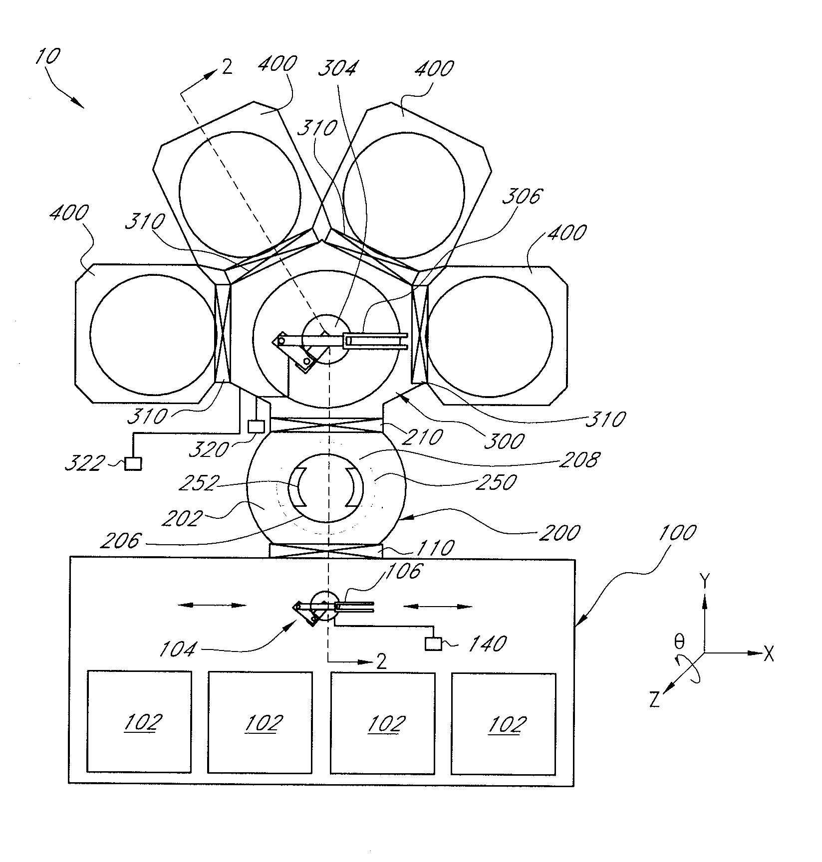
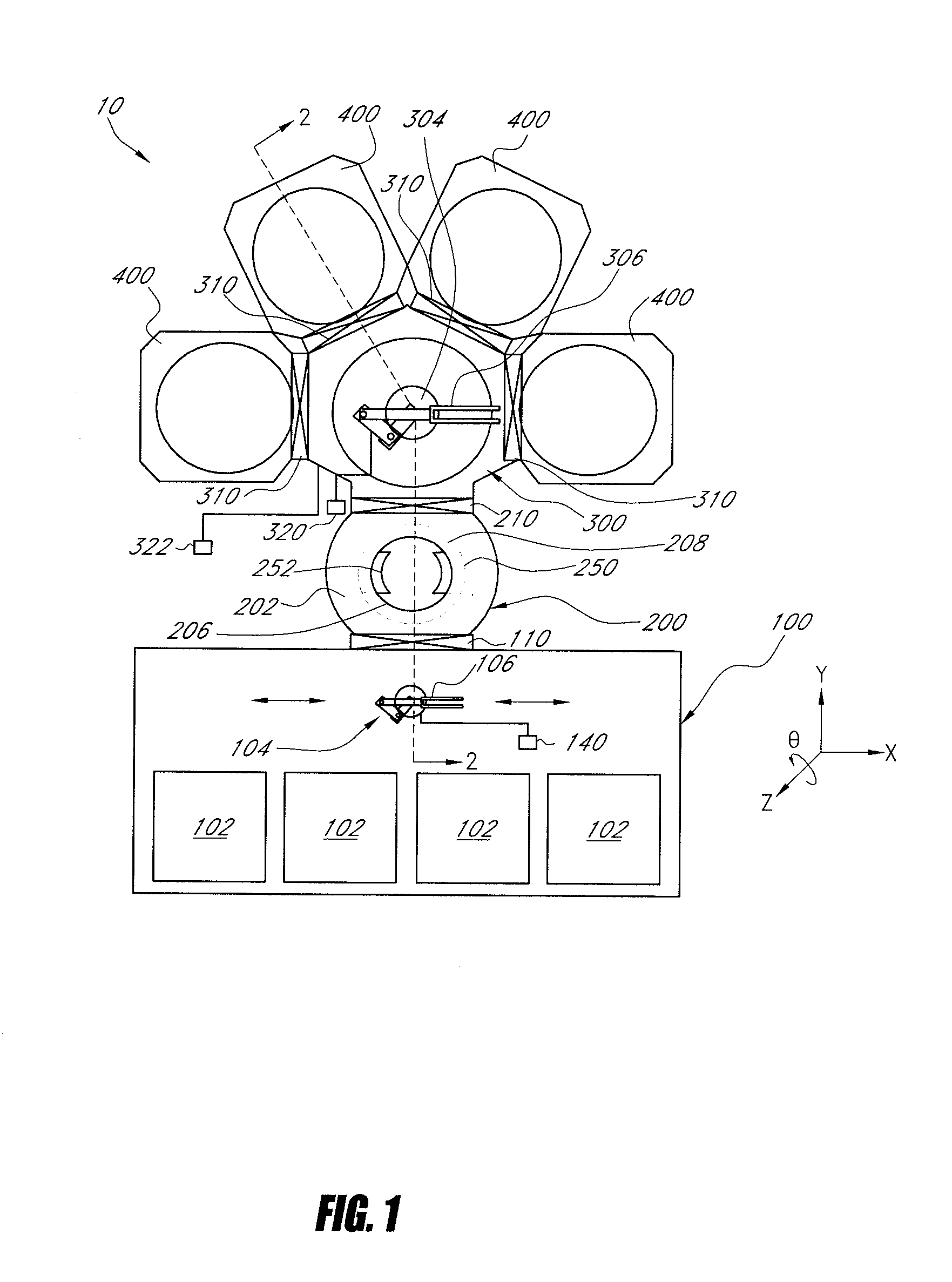
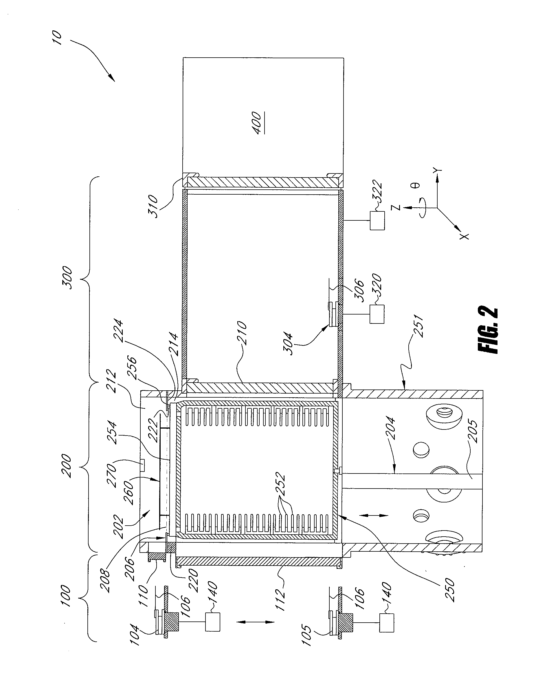
[0021]Referring to FIG. 1, a schematic plan view of an example embodiment of a semiconductor processing apparatus 10 is shown. The illustrated semiconductor processing apparatus 10 includes a loading station 100, a load lock 200, a workpiece handling chamber 300, and a plurality of process modules 400.
[0022]As shown in FIGS. 1-2, the loading station 100 is the location at which wafers 11 (FIG. 3A) are introduced or withdrawn from the semiconductor processing apparatus 10. The terms “semiconductor wafer” and / or “wafer” as used herein may refer to a substrate as it may exist in any of the various stages of the semiconductor fabrication process or may refer to a substrate that is used to validate a semiconductor fabrication process. The loading station 100 can be exposed to the ambient environment, for example the clean room environment external to the semiconductor processing apparatus 10, or can be a closed and purged environment. In some embodiments, the loading station 100 is at at...
PUM
| Property | Measurement | Unit |
|---|---|---|
| Temperature | aaaaa | aaaaa |
| Flow rate | aaaaa | aaaaa |
| Heat | aaaaa | aaaaa |
Abstract
Description
Claims
Application Information