Detection circuit and method for a liquid crystal display

a detection circuit and liquid crystal display technology, applied in the direction of instruments, computing, electric digital data processing, etc., can solve the problems of difficult to discriminate the display effects of the damaged area of the alignment film and the normal area, and the abnormal display is difficult to distinguish the display effect of the damaged area

Active Publication Date: 2010-09-02
BEIJING BOE OPTOELECTRONCIS TECH CO LTD
View PDF10 Cites 10 Cited by
  • Summary
  • Abstract
  • Description
  • Claims
  • Application Information

AI Technical Summary

Benefits of technology

[0007]The embodiments of present invention aim to address the problems of the prior art, provide a detection circuit and a detection method for the liquid crystal display, therefore resolves the problem in the prior art that it is difficult for the operator to recognize a white dot of the damaged area of alignment film and easily resulting the issue of missing detection.
[0025]The pixel voltage signal is generated by the continuous high level signal and continuous low level signal of the signal source in the technical solution of the present invention, and said pixel voltage signal could form a polarity inversion mode of column inversion, when compared with the polarity inversion mode of row inversion in the prior art, the embodiments of present invention change the mutual affection and crosstalk interference of the signals between neighboring liquid crystal molecules, such that the white dot of the damaged area of alignment film is more prominent during the detection process, so it would be easy for the operator to recognize it and thus avoid the issue of missing detection.

Problems solved by technology

In case of damage to the alignment film, the normal orientation angle and pre-tilt angle of the alignment film no longer exist, which causes turbulence to the liquid crystal molecules, so that the liquid crystal molecules could not produce optical rotation effect controlled by the voltage on both ends of the pixels electrode as in the normal situation, thus resulting in the light leaking phenomenon, which would cause abnormal display in the damaged area of the alignment film, and white dot occurs.
However, because the damage to the alignment film normally happens in a very small area, such as in the area of the 9 sub-pixel shown in FIG. 1, and there are glutinosity effect or crosstalk interference of the signals between liquid crystal molecules in said area and liquid crystal molecules of the surrounding normal areas, and the selectivities to the light through the upper and lower polarization sheets (the polarization directions are orthogonal), there is a problem that it is difficult to discriminate the display effects of the damaged area of the alignment film and the normal area, for example, it is difficult to discriminate the display effects of the damaged area and the normal area under the above described two rows polarity inversion mode and single row polarity inversion mode.
Therefore, in the detection process, it is difficult for the operator to recognize the white dot of the damaged area of alignment film, and missing detection easily occurs.

Method used


Image

  • Detection circuit and method for a liquid crystal display
  • Detection circuit and method for a liquid crystal display
  • Detection circuit and method for a liquid crystal display

Examples


first embodiment

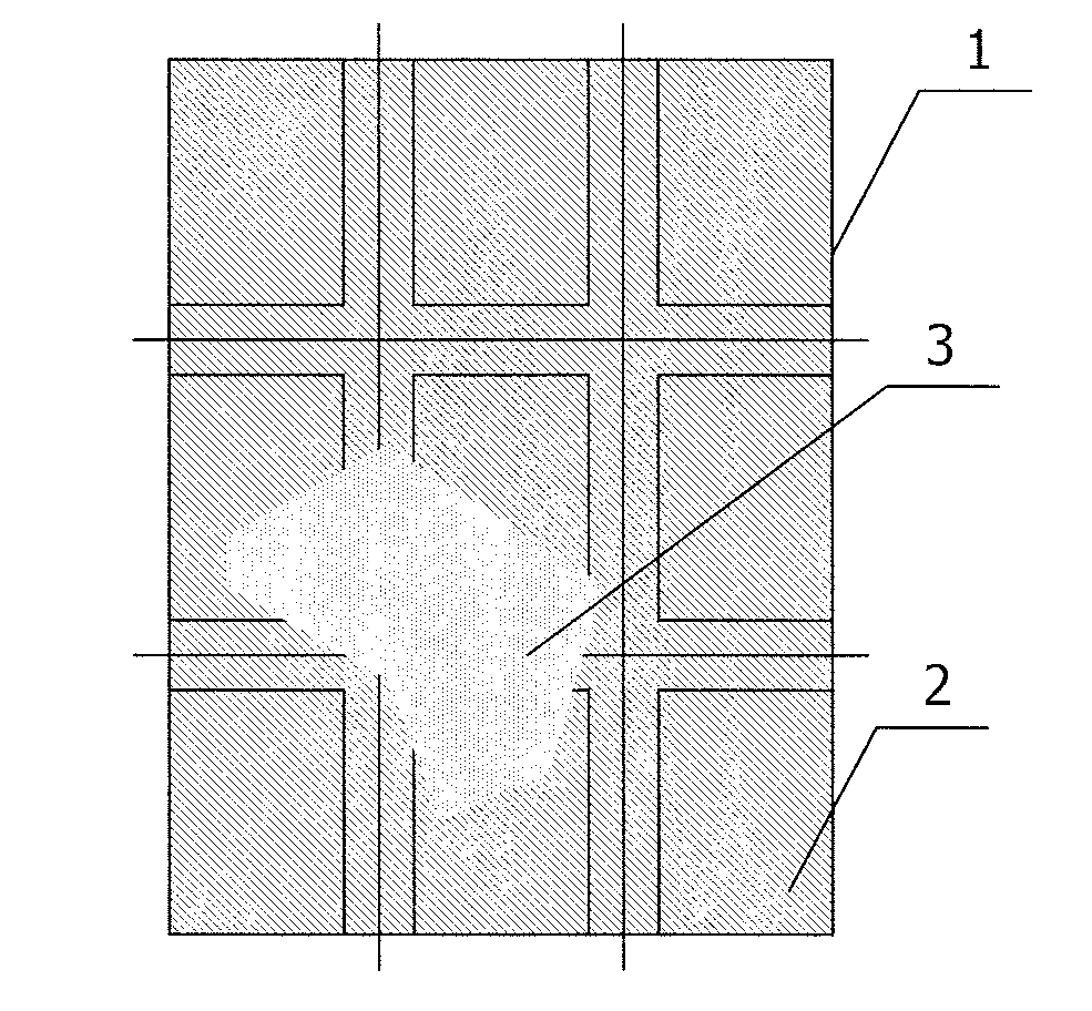
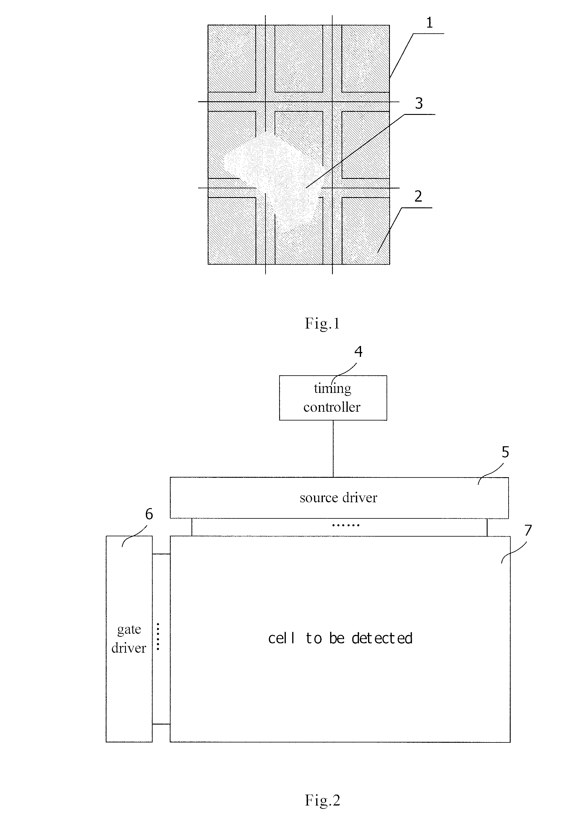
[0042]FIG. 7 is an illustrative diagram of the structure of a detection circuit for a liquid crystal display according to the present invention. Referring to FIG. 7, said detection circuit includes a source driver 5, a gate driver 6 and a signal source 8. In order to describe the technical solution of the present embodiment more clearly, FIG. 7 also shows a cell 7 to be detected that is connected to the detection circuit. The gate driver 6 provides a row scan signal to the cell 7 to be detected; the signal source 8 provides a polarity inversion signal to the source driver 5, the polarity inversion signal includes a continuous high level signal and a continuous low level signal; the source driver 5 performs a digital-analogue conversion on the received display data signal according to a preset reference voltage and the polarity inversion signal, generates a pixel voltage signal, and sends the pixel voltage signal to the cell 7 to be detected, wherein the polarity inversion mode forme...

second embodiment

[0058]FIG. 13 is a flowchart of a detection method for the liquid crystal display according to the present invention, as illustrate in FIG. 13, the detection method of the present embodiment can be based on the detection circuit of FIG. 11, as illustrate in FIG. 13, and particularly, the detection method comprises:

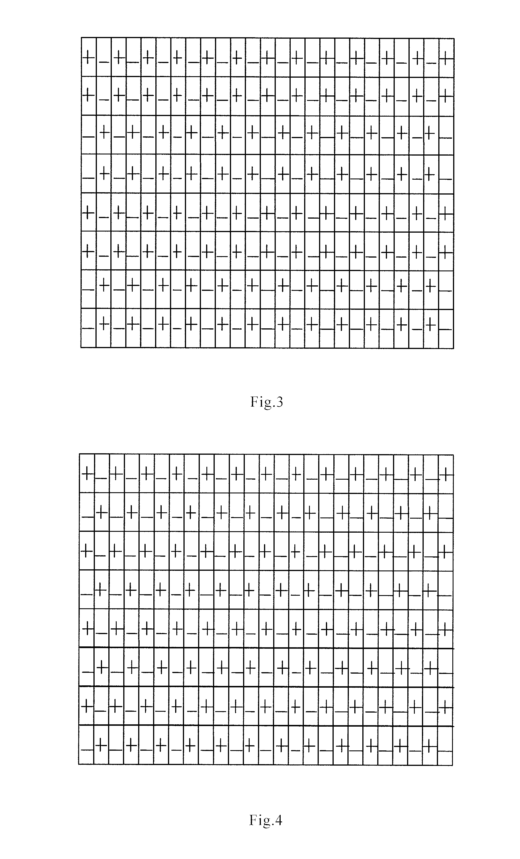
[0059]step 201, timing controller provides a polarity inversion signal to the source driver, the polarity inversion signal is a periodical square wave signal. At this time, the control switch is not depressed, the timing controller and the source driver are in a connection state.

[0060]Step 202, the source driver performs a digital-analogue conversion on the received display data signal according to a preset reference voltage and the polarity inversion signal provided by the timing controller, so as to generate a pixel voltage signal.

[0061]Step 203, gate driver provides a row scan signal to the liquid crystal cell to be detected, and under the control of said row scan signa...


PUM


Abstract

A detection circuit and a detection method for liquid crystal display are provided. The detection circuit comprises gate driver for providing row scan signal to liquid crystal cell to be detected; signal source for providing polarity inversion signal to source driver, polarity inversion signal comprises continuous high level signal and continuous low level signal; source driver for performing digital-analogue conversion on received display data signal according to preset reference voltage and polarity inversion signal, generating pixel voltage signal, and sending pixel voltage signal to liquid crystal cell to be detected, polarity inversion mode formed by pixel voltage signal is column inversion mode. The polarity inversion mode of column inversion, formed by pixel voltage signal in technical solution makes white dot of damaged area of alignment film is more prominent during detection process, so it would be easy for the operator to recognize it and avoid the issue of missing detection.

Description

BACKGROUND[0001]1. Field of the Invention[0002]The embodiments of present invention relate to a detection circuit and a detection method for a liquid crystal display.[0003]2. Discussion of the Background[0004]In the structure of a liquid crystal display, an alignment film may control liquid crystal molecules to produce optical rotation, wherein its orientation angle and pre-tilt angle are critical conditions enabling the liquid crystal molecules to produce optical rotation. The manufacture procedure of the alignment film includes the processes of coating and rubbing alignment film, bubbles generated in coating process and broken after rubbing process and rubbing scratches caused by particles and foreign matters and so on during the rubbing process would cause the alignment film being partially damaged, as illustrated in FIG. 1. FIG. 1 is an illustrative diagram of the alignment film formed after the rubbing process, alignment film 2 is formed on a pixel area 1 of a substrate in FIG....

Claims


Application Information

Patent Timeline
Patent Type & Authority Applications(United States)
IPC IPC(8): G06F3/038
CPCG09G3/006G09G3/3648G09G3/3614G09G2330/10G06F3/038G09G3/3406G09G2300/0439G09G2310/08
Inventor PENG, ZHILONGHE, XIANGFEIWANG, WEI
Owner BEIJING BOE OPTOELECTRONCIS TECH CO LTD
Why Eureka
Try Eureka