

Photoreceptor, Method Of Manufacturing Same, Image Formation Method, Image Forming Apparatus, And Process Cartridge
a technology of photoreceptor and manufacturing method, which is applied in the direction of electrophotography process apparatus, corona discharge, instruments, etc., can solve the problems of abnormal images, increased contact pressure between cleaning blade and photoreceptor, and prone to abraded organic photoconductor repetitively used in electrophotography process, etc., to achieve good electrical characteristics, high and stable abrasion resistance and damage resistan
- Summary
- Abstract
- Description
- Claims
- Application Information
AI Technical Summary
Benefits of technology
Problems solved by technology
Method used
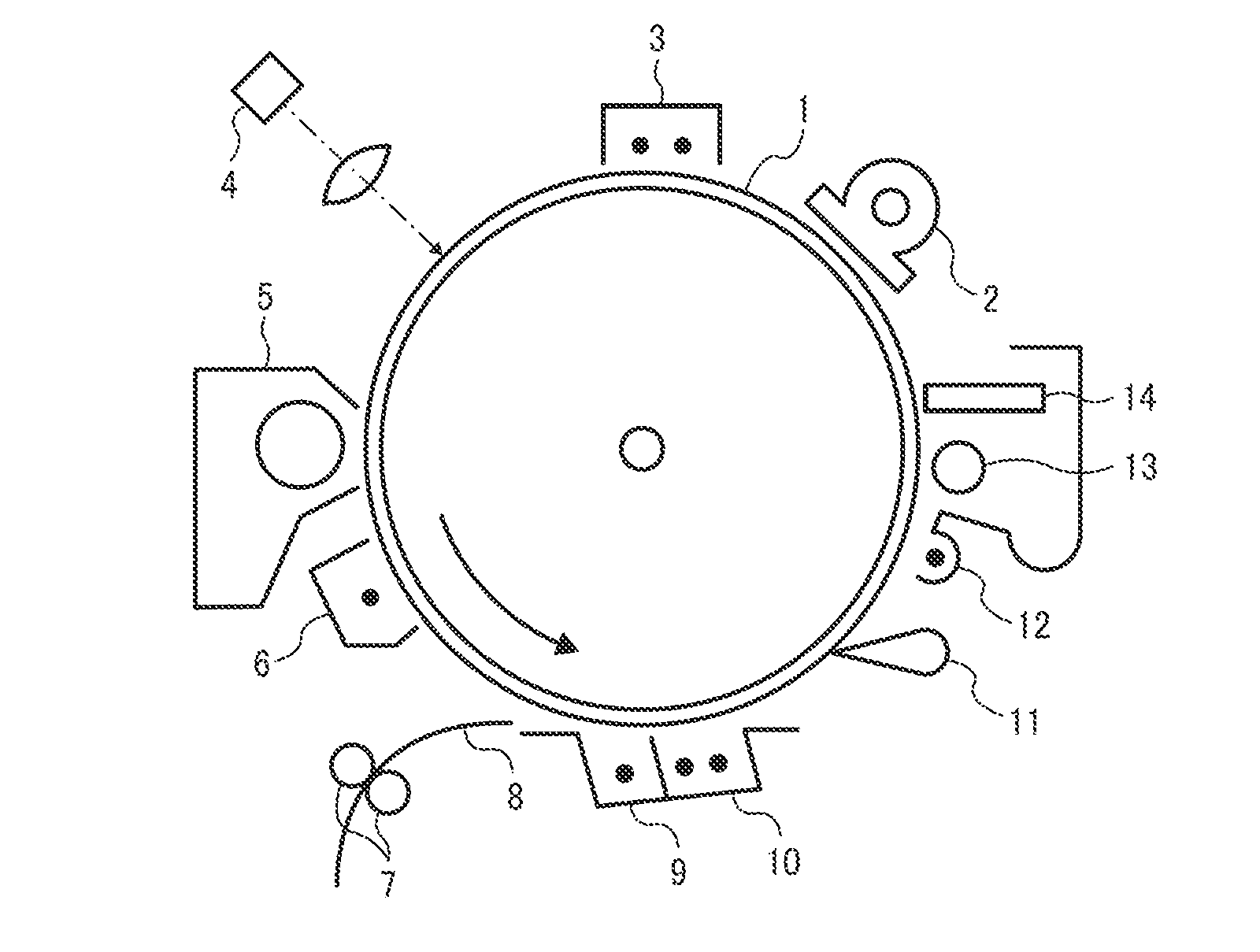
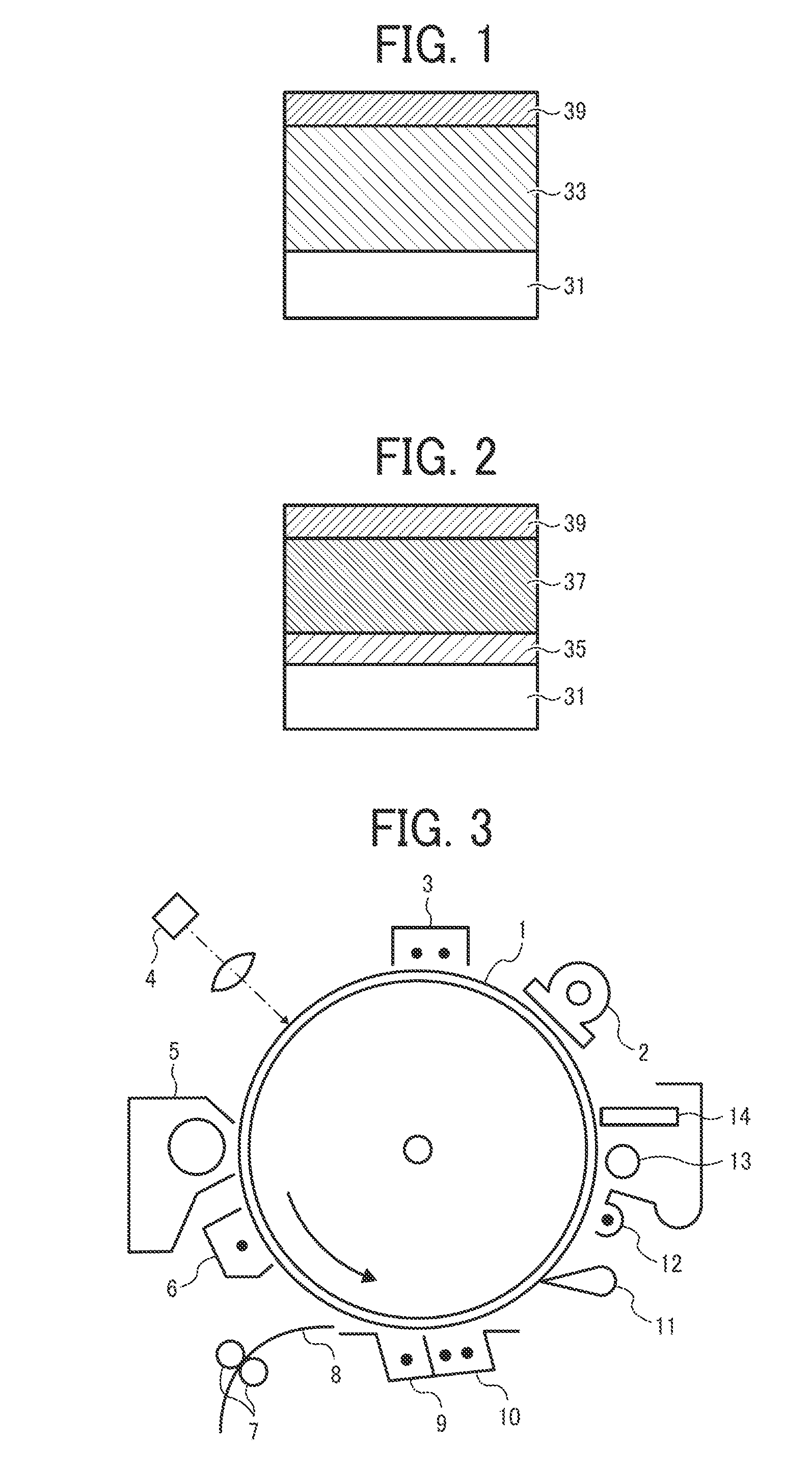
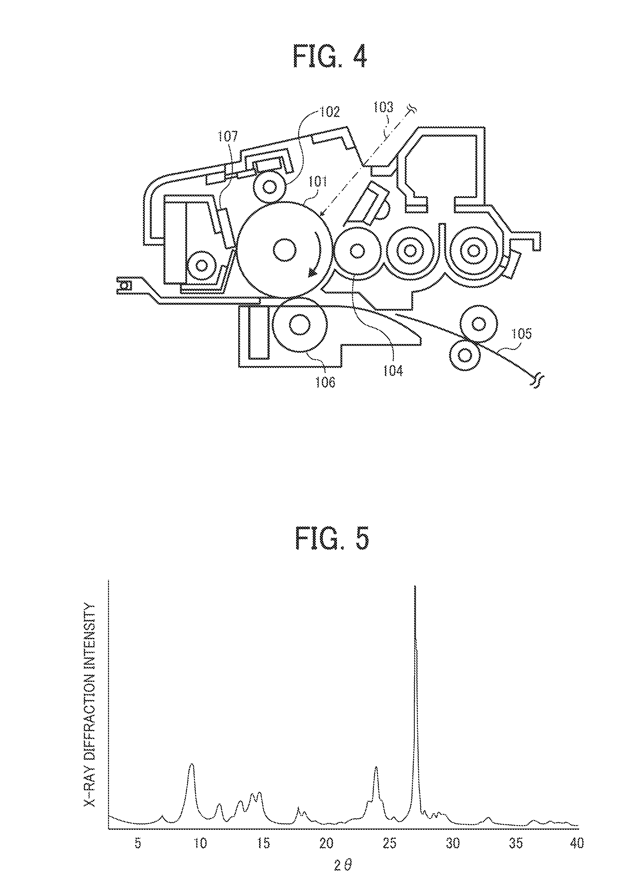
Image

Examples
example 1
[0252]Liquid application having the following recipe is applied to an aluminum substrate (outer diameter: 100 mm φ) by a dip coating method to form an undercoating layer having a layer thickness of 4.0 μm after drying.
Liquid Application for Undercoating LayerAlkyd resin (Beckozole 307-60-EL, manufactured by6.5 partsDainippon Ink and Chemicals, Inc.; Solid portion: 50%)Melamine resin (Super-beckamine G-821-60, manufactured by3.5 partsDainippon Ink and Chemicals, Inc.)Titanium oxide (CR-El, manufactured by Ishiahara Sangyo 60 partsKaisha Ltd.)Methylethylketone 90 parts
[0253]Liquid application for charge generation layer containing the titanyl phthalocyanine pigment is applied to the undercoating layer by a dip coating followed by heating and drying to form a charge generation layer having a layer thickness of 0.3 μm.
Liquid Application for Charge Generation LayerTitanyl phtahlocyanine pigment manufactured by Synthesis2.5 partsExample 1Polyvinylbutyral (BX-1, manufactured by Sekisui0.5 ...
example 2
[0260]The liquid application of surface layer is prepared in the same manner as in Example 1 except that the radical polymerizable monomer having at least 3 functional groups with no charge transport structure for use in the liquid application of surface layer is replaced with a TMPTA (V#295, manufactured by Osaka Organic Chemical Industry Ltd.). The sulfur concentration contained in the TMPTA after refinement is 30 ppmw. The sulfur concentration remaining in the surface layer is 15 ppmw. A mutation test is conducted for the TMPTA refined by the column chromatography and its colony increase multiple is 1.1.
example 3
[0261]The liquid application of surface layer is prepared in the same manner as in Example 1 except that the radical polymerizable monomer having at least 3 functional groups with no charge transport structure for use in the liquid application of surface layer is replaced with a TMPTA (kayarad, manufactured by Nipponn Kayaku Co., Ltd.) The sulfur concentration of the product prior to refinement is 310 ppmw. The sulfur concentration contained in the TMPTA after refinement is 30 ppmw. The sulfur concentration remaining in the surface layer is 20 ppmw. A mutation test is conducted for the TMPTA refined by the column chromatography and its colony increase multiple is 1.2.
PUM
 Abstract
Description
Claims
Application Information