

Active array substrate, liquid crystal display panel and method for driving the same
a technology of liquid crystal display panel and active array substrate, which is applied in the direction of non-linear optics, static indicating devices, instruments, etc., can solve problems such as color washout, and achieve the effect of low gray level
- Summary
- Abstract
- Description
- Claims
- Application Information
AI Technical Summary
Benefits of technology
Problems solved by technology
Method used
Image

Examples
first embodiment
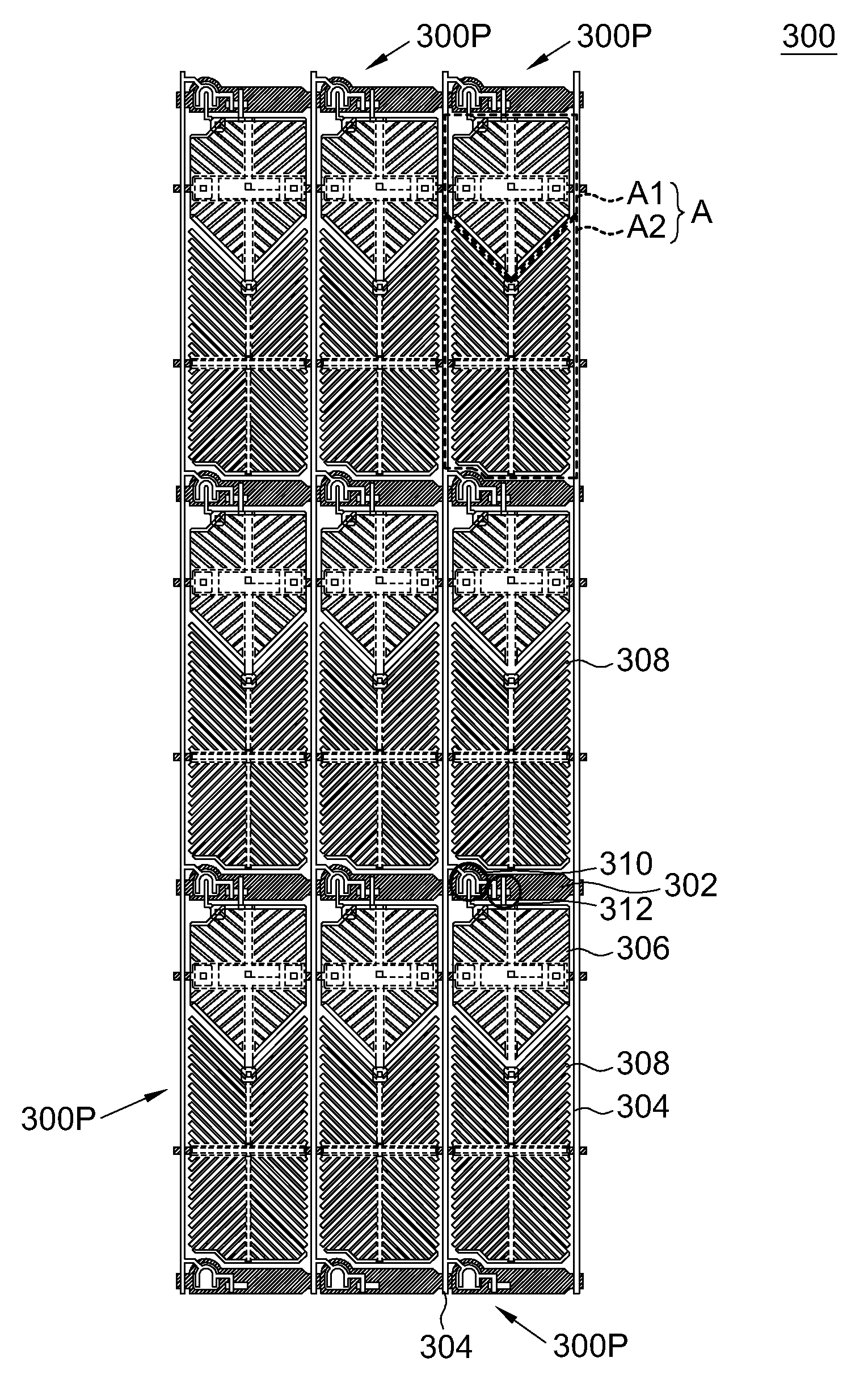
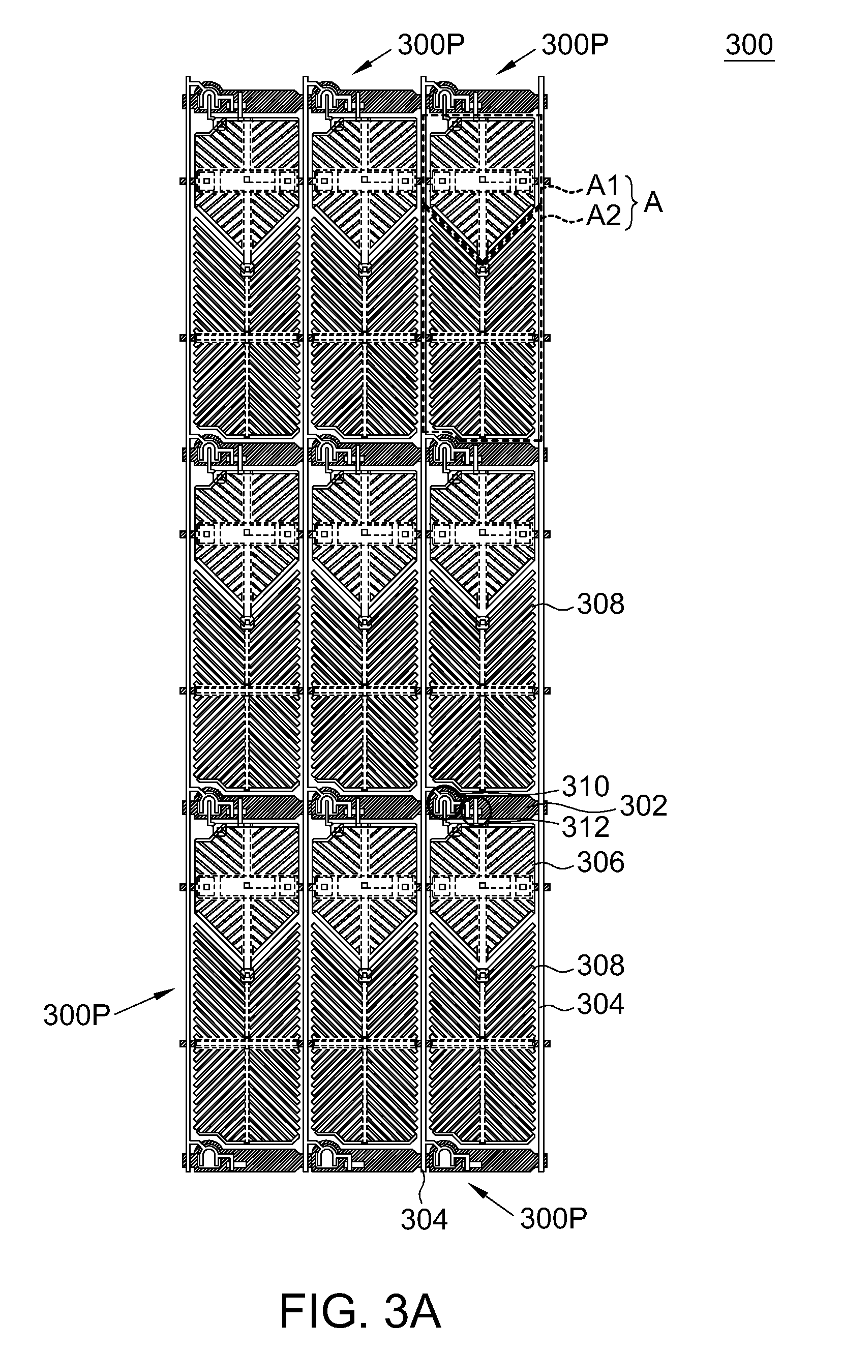
[0041]FIG. 3A is a top view of an active array substrate according to the first embodiment of the present invention. FIG. 3B shows an equivalent circuit of a pixel area of the active array substrate 2 incorporated with the opposite substrate according to the first embodiment of the present invention. FIG. 3C is an enlarged top view of a pixel according to the first embodiment of the present invention. FIG. 3D is a cross section view along line I-I′ in FIG. 3C. FIG. 3E is a cross section view along line II-II′ in FIG. 3C.
[0042]In FIGS. 3A and 3B, active array substrate 300 includes base (not shown), scan lines 302, data lines 304, pixel units 3000, first common electrode 320 and second common electrode 340. For explanation, only 9 pixels 300P are shown, but not limited thereto. Scan lines 302 are disposed on the base. Data lines 304 are disposed on the base and substantially perpendicular with the scan lines 302. Pixel units 3000 are electrically connected with corresponding scan lin...
second embodiment
[0052]FIG. 4A is a top view of an active array substrate according to the second embodiment of the present invention. FIG. 4B shows an equivalent circuit of a pixel area of the active array substrate incorporated with the opposite substrate 2 according to the second embodiment of the present invention. FIG. 4C is an enlarged top view of a pixel according to the second embodiment of the present invention. FIG. 4D is a cross section view along line I-I′ in FIG. 4C. FIG. 4E is a cross section view along line II-II′ in FIG. 4C.
[0053]In FIGS. 4A and 4B, active array substrate 400 includes base (not shown), scan lines 402, data lines 404, pixel units 4000, first common electrode 420 and second common electrode 440. For explanation, only 9 pixels 400P are shown, but not limited thereto. Scan lines 402 are disposed on the case. Data lines 404 are disposed on the base and substantially perpendicular with the scan lines 402. Pixel units 4000 are electrically connected with corresponding scan ...
third embodiment
[0062]FIG. 5A is a top view of an active array substrate according to the third embodiment of the present invention. FIG. 5B shows an equivalent circuit of a pixel area of the active array substrate 2 incorporated with the opposite substrate according to the third embodiment of the present invention. FIG. 5C is an enlarged top view of a pixel according to the third embodiment of the present invention. FIG. 5D is a cross section view along line I-I′ in FIG. 5C. FIG. 5E is a cross section view along line II-II′ in FIG. 5C.
[0063]In FIGS. 5A and 5B, active array substrate 500 includes base (not shown), scan lines 502, data lines 504, pixel units 5000, first common electrode 520 and second common electrode 540. For explanation, only 9 pixels 500P are shown, but not limited thereto. Scan lines 502 are disposed on the case. Data lines 504 are disposed on the base and substantially perpendicular with the scan lines 502. Pixel units 5000 are electrically connected with corresponding scan lin...
PUM
| Property | Measurement | Unit |
|---|---|---|
| width | aaaaa | aaaaa |
| width | aaaaa | aaaaa |
| width | aaaaa | aaaaa |
Abstract
Description
Claims
Application Information