Zero voltage switching high-frequency inverter

a high-frequency inverter, zero-voltage technology, applied in the direction of electric variable regulation, process and machine control, instruments, etc., can solve the problems of large surge current, large surge voltage, and large surge current, and suppress so as to achieve high efficiency and suppress the effect of the conduction loss of the switch

Inactive Publication Date: 2010-10-14
TOKYO UNIV OF MANNE SCI & TECH
View PDF3 Cites 1 Cited by
  • Summary
  • Abstract
  • Description
  • Claims
  • Application Information

AI Technical Summary

Benefits of technology

[0044]In other words, since the present invention is capable of decreasing the number of capacitors as constituent elements of a circuit, while ensuring the zero-voltage switching, the present invention enables a reduction in costs and a simple circuit structure.
[0046]As a result, a highly efficient high-frequency inverter can be provided which can suppress a conduction loss of the switches by means of the large amplitude operation of the load current, with the main switch current being suppressed.

Problems solved by technology

In a high-frequency inverter, there generates a switching loss, a large surge voltage, and a large surge current, with an increase in frequency.
As a result of the current flows with the voltage being applied, the product of the current and the voltage becomes a power loss.
These switching loss, surge voltage, and surge current result in the loss of energy, and sometimes damage a switch.
Under this state, although a switching loss can be reduced due to the ZVS, a conduction loss is disadvantageously increased by the current of large amplitude that flows through the switches, when the switches are on.
Further, in both the conventional series resonance half-bridge ZVS high-frequency inverter with two switches and the conventional series resonance full-bridge ZVS high-frequency inverter with four switches, each of the switches is provided with a capacitor, which entails a complicated circuit structure.

Method used


Image

  • Zero voltage switching high-frequency inverter
  • Zero voltage switching high-frequency inverter
  • Zero voltage switching high-frequency inverter

Examples


Embodiment Construction

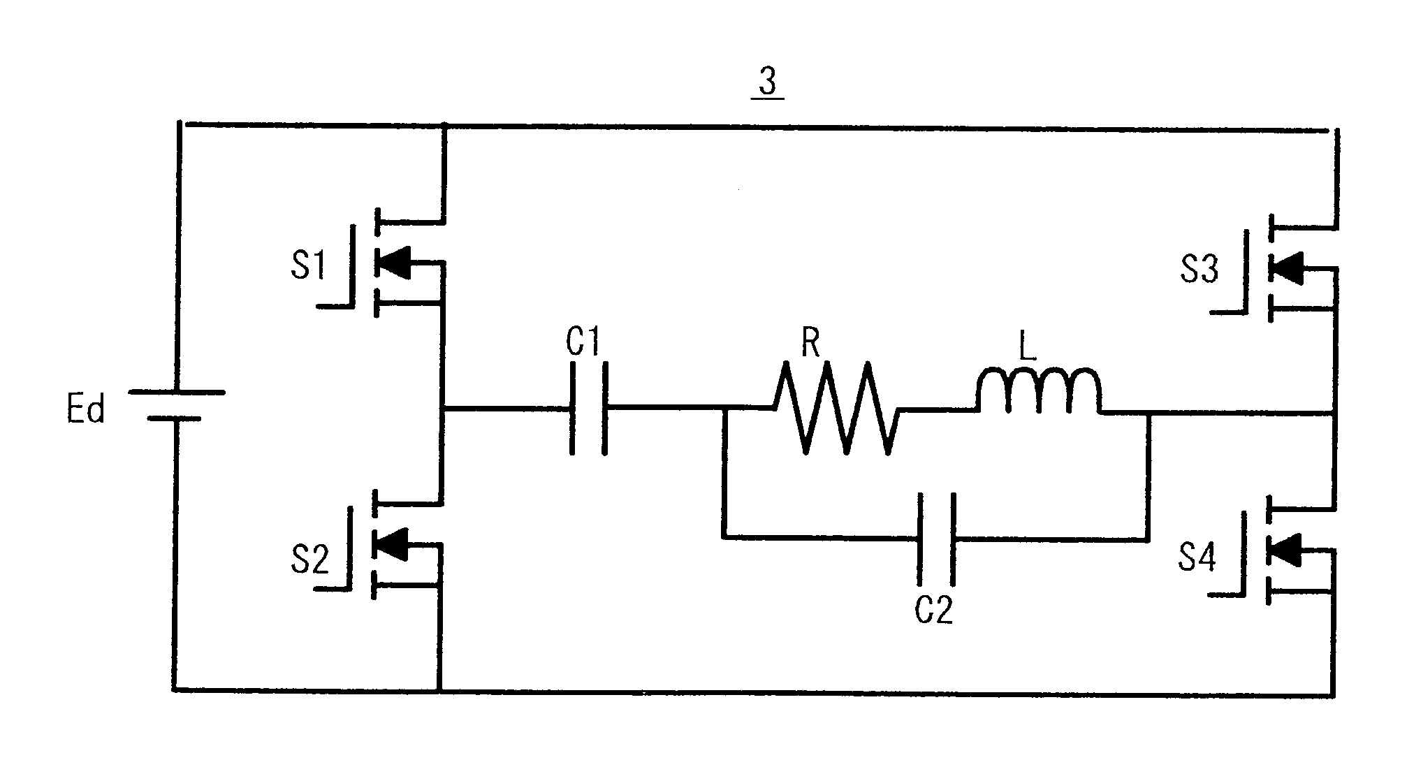
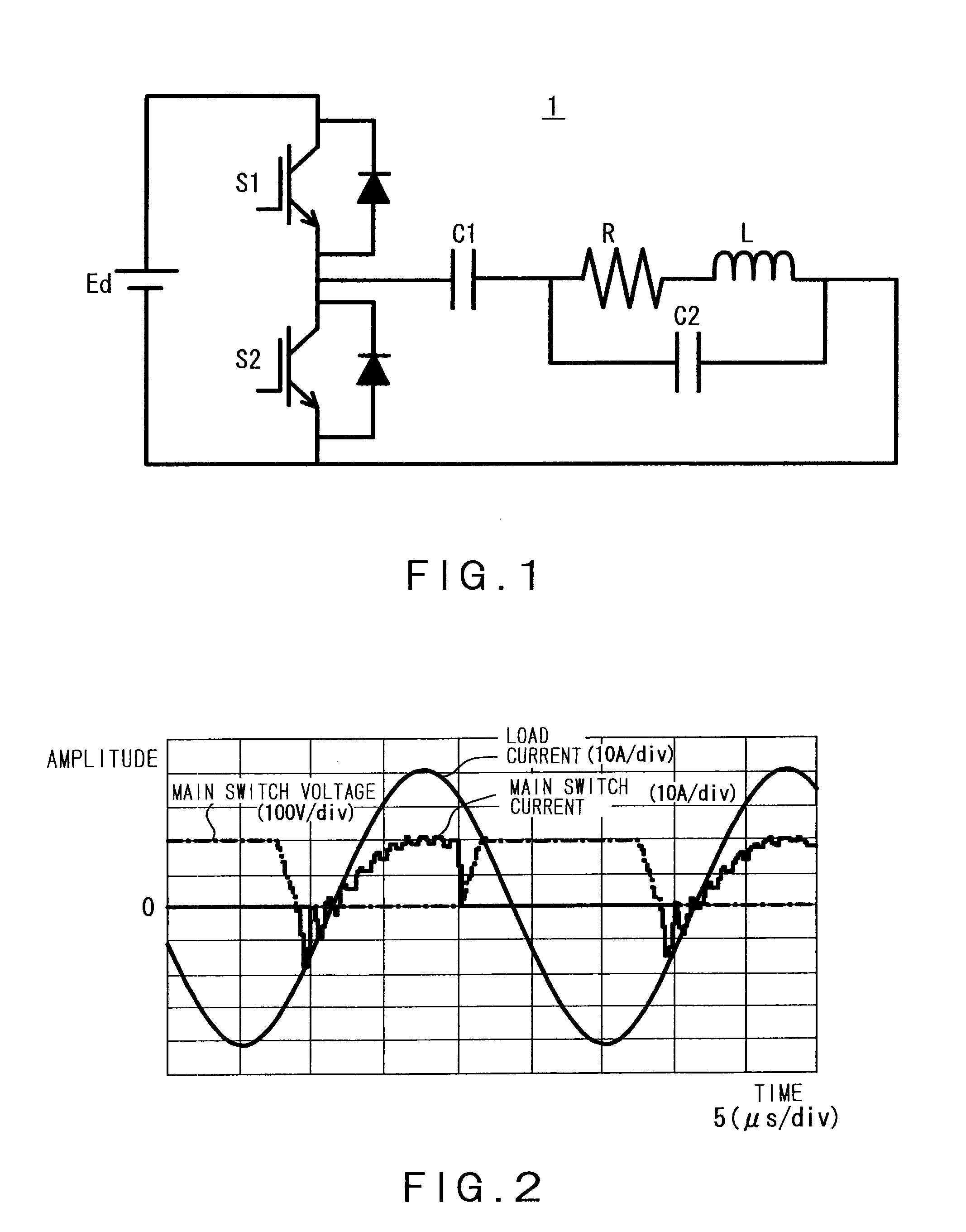
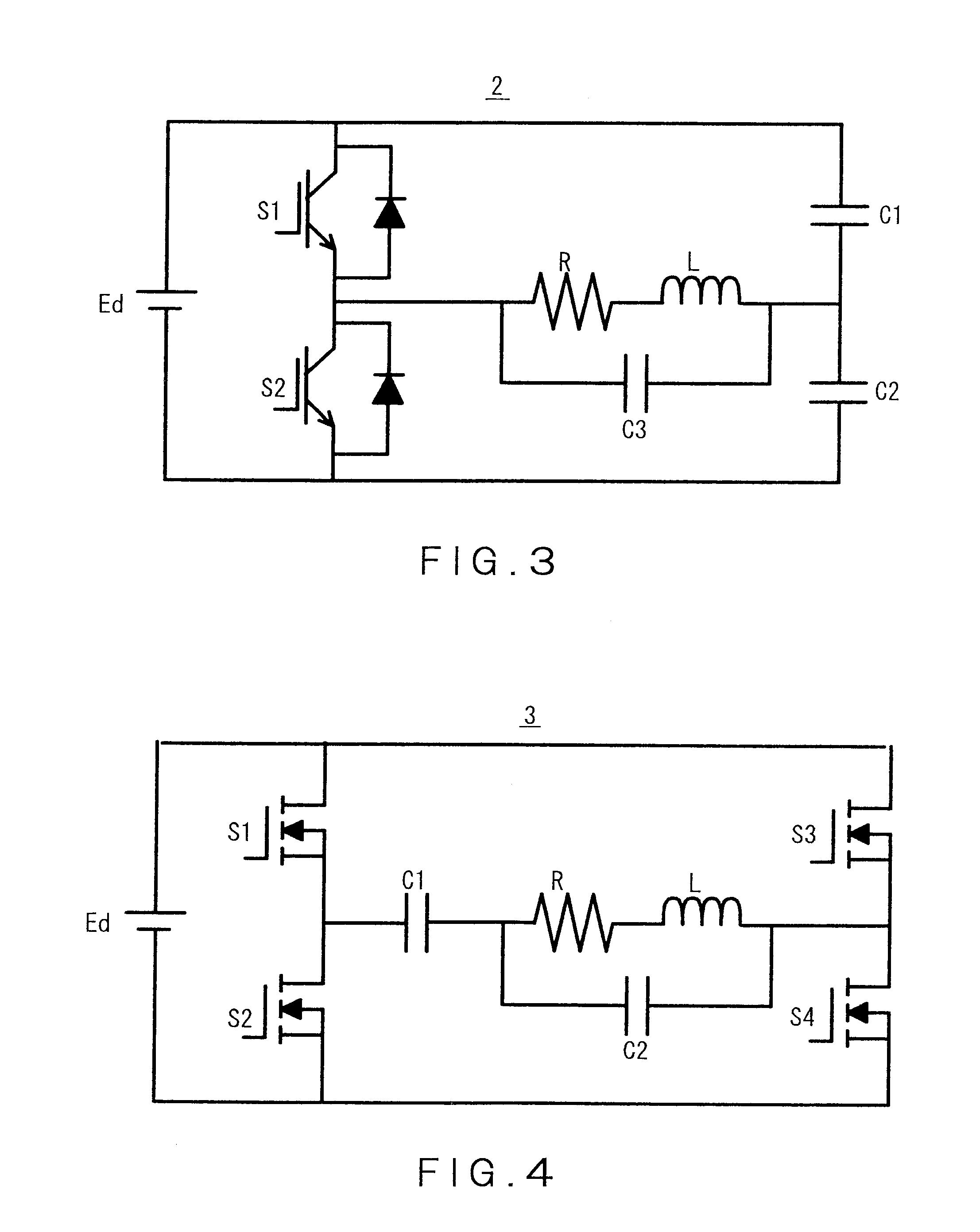
[0054]FIG. 1 shows a “half-bridge zero-voltage switching high-frequency inverter with two switches (half-bridge ZVS high-frequency inverter with two switches)” in one embodiment of the present invention.

[0055]As shown in FIG. 1, the half-bridge ZVS high-frequency inverter 1 with two switches in this embodiment includes: a first switch S1 and a second switch S2 which are connected in series between power sources Ed; a first capacitor C1, an impedance element R, and an inductor element L which are connected in series between a connecting path connecting the first switch S1 and the second switch S2 and one end of the power sources Ed; and a second capacitor C2 connected in parallel to the impedance element R and the inductor element L.

[0056]The “one end of the power sources Ed” may either be a positive electrode side or a negative electrode side.

[0057]The first switch S1 and the second switch S2 are formed of a transistor and a diode, respectively. Not limited to IGBTs, the first switc...


PUM


Abstract

There is provided a zero-voltage switching high-frequency inverter capable of supplying a current of a large amplitude operation to a load, while suppressing a main switch current. The zero-voltage switching high-frequency inverter according to the present invention comprises: a first switch S1 and a second switch S2 that are connected in series between power sources Ed; a first capacitor C1, an impedance element R, and an inductor element L that are connected in series between a connecting path connecting the first switch S1 and the second switch S2 and one end of the power sources Ed; and a second capacitor C2 connected in parallel to the impedance element R and the inductor element L that are connected in series.

Description

[0001]This application is a division of U.S. application Ser. No. 11 / 573,827, filed on Feb. 16, 2007, the entire contents of which is incorporated by reference. U.S. application Ser. No. 11 / 573,827 is a national phase application of PCT / JP05 / 002249 under 35 U.S.C §371, filed on Feb. 15, 2005, which claims the benefit of priority of Japanese Patent Application No. 2004-236446, filed on Aug. 16, 2004.BACKGROUND OF THE INVENTION [0002]1. Field of the Invention[0003]The present invention relates to a zero-voltage switching (ZVS) high-frequency inverter.[0004]More particularly, the present invention relates to a zero-voltage switching (ZVS) high-frequency inverter having a simpler structure than that of a conventional one. When a load resistance value is low, the ZVS high-frequency inverter of the present invention allows a larger electric current to flow through a load, as compared with an electric current flowing through a switch.[0005]2. Background Art[0006]In a high-frequency inverte...

Claims


Application Information

Patent Timeline
Patent Type & Authority Applications(United States)
IPC IPC(8): H02M7/537
CPCH02M7/538Y02B70/1441H02M2007/4815H02M7/4815Y02B70/10
Inventor HATANAKA, YOSHIHIRO
Owner TOKYO UNIV OF MANNE SCI & TECH
Why Eureka
Try Eureka