Semiconductor device and method of manufacturing the same

Inactive Publication Date: 2010-11-04
FUJIKURA LTD
View PDF1 Cites 15 Cited by
  • Summary
  • Abstract
  • Description
  • Claims
  • Application Information

AI Technical Summary

Benefits of technology

[0017]According to the present invention, after the first and second substrates are bonded to each other, at least one of the substrates is thinned, and then, the cavity is formed. This makes it possible to prevent irregularities or cracks caused by the presence or absence of the cavity after the grinding, and therefore it is possible to more regularly and thinly grind the wafer. This also makes it possible to reduce the thickness of the package in comparison with that of the related art. As a result, according to the present invention, it is possi

Problems solved by technology

However, when a wafer-level package is manufactured using this method, since the thinning is performed by grinding the substrate after bonding in which the cavity is already formed, the weight applied during grinding is different between portions where the cavi

Method used


Image

  • Semiconductor device and method of manufacturing the same
  • Semiconductor device and method of manufacturing the same
  • Semiconductor device and method of manufacturing the same

Examples


Example

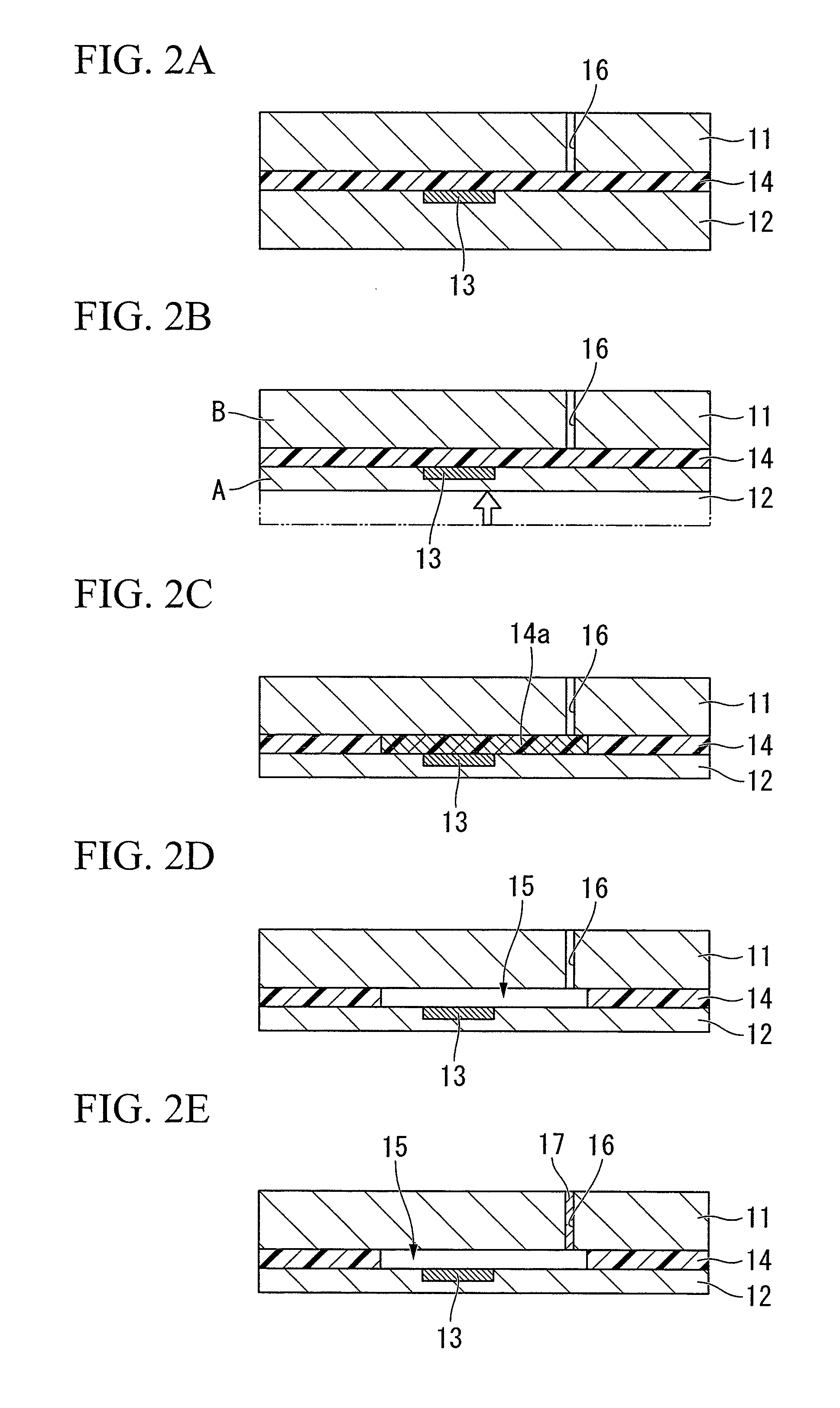
[0040]A first embodiment of the present invention will be described.

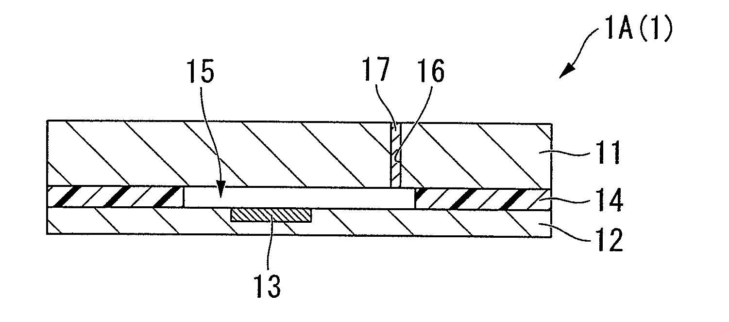
[0041]FIG. 1 is a schematic cross-sectional view illustrating an example of a semiconductor device according to the present invention.

[0042]The semiconductor device 1A(1) includes a first substrate 11 with optical transparency, a second substrate 12 which has a surface on which a functional element 13 is provided and which is bonded to the first substrate 11 such that the functional element 13 faces the first substrate 11, a cavity 15 arranged in a portion corresponding to the functional element 13 at a bonding portion between the first and second substrates 11 and 12, a through-hole 16 communicated with the cavity 15, and a sealing portion 17 for sealing the cavity 15 and the through-hole 16.

[0043]In the semiconductor device 1A, the first and second substrates 11 and 12 are bonded to each other by photosensitive resin 14.

[0044]In the semiconductor device 1A according to the present invention, the substrate is more ...

Example

Second Embodiment

[0075]Next, a second embodiment of the present invention will be described.

[0076]FIG. 3 is a schematic cross-sectional view illustrating another example of a semiconductor device according to the present embodiment.

[0077]The semiconductor device 1B(1) includes a first substrate 21 with optical transparency, a second substrate 22 which has a surface on which a functional element 23 is provided and which is bonded to the first substrate 21 such that the functional element 23 faces the first substrate 21, a cavity 24 arranged in a portion corresponding to the functional element 23 at a bonding portion between the first and second substrates 21 and 22, a through-hole 25 communicated with the cavity 24, and a sealing portion 26 for sealing the cavity 24 and the through-hole 25.

[0078]In the semiconductor device 1B according to the present invention, it is possible to prevent irregularities or cracks caused by the presence or absence of the cavity 24 and more regularly thi...


PUM


Abstract

A method of manufacturing a semiconductor device includes: a bonding step of bonding a first substrate with optical transparency and a second substrate having a surface on which a functional element is provided to each other such that the functional element faces the first substrate; a thinning step of thinning at least one of the first and second substrates; and a through-hole forming step of forming a cavity and a through-hole communicated with the cavity in at least part of a bonding portion between the first and second substrates. According to the present invention, it is possible to prevent irregularities or cracks caused by the presence or absence of the cavity and more regularly thin the substrate. In addition, it is possible to manufacture a semiconductor device capable of contributing to the miniaturization of devices and electronic equipment having the devices, using a more convenient process.

Description

TECHNICAL FIELD[0001]The present invention relates to a semiconductor device which allows for a package such as an image sensor or a MEMS (Micro Electro Mechanical System) device to be miniaturized and made thinner, and a method of manufacturing the same. Priority is claimed on Japanese Patent Application No. 2007-331695, filed Dec. 25, 2007, the content of which is incorporated herein by reference.BACKGROUND ART[0002]With the increasing miniaturization and sophistication of electrical equipment such as mobile phones in recent years, it is demanded that the electronic devices used therein also be miniaturized. In order to meet these demands, it is indispensable to develop technologies for increasing the miniaturization and sophistication of device package, in addition to the miniaturization of the device itself. For technologies that achieve the miniaturization of the device package, various device packages employing a wafer-level package technology have been proposed, and it is exp...

Claims


Application Information

Patent Timeline
IPC IPC(8): H01L29/84H01L21/50H01L31/0203
CPCB81C1/00317B81C2203/0118B81C2203/0145H01L27/14618B81C2201/0104H01L27/14683B81C2201/0125B81C2201/0108H01L27/14627H01L2924/0002H01L2924/00
Inventor YAMAMOTO, SATOSHIHASHIMOTO, HIROKAZU
Owner FUJIKURA LTD
Why Eureka
Try Eureka