

Lighting device, display, and method for manufacturing the same
- Summary
- Abstract
- Description
- Claims
- Application Information
AI Technical Summary
Benefits of technology
Problems solved by technology
Method used
Image

Examples
first embodiment
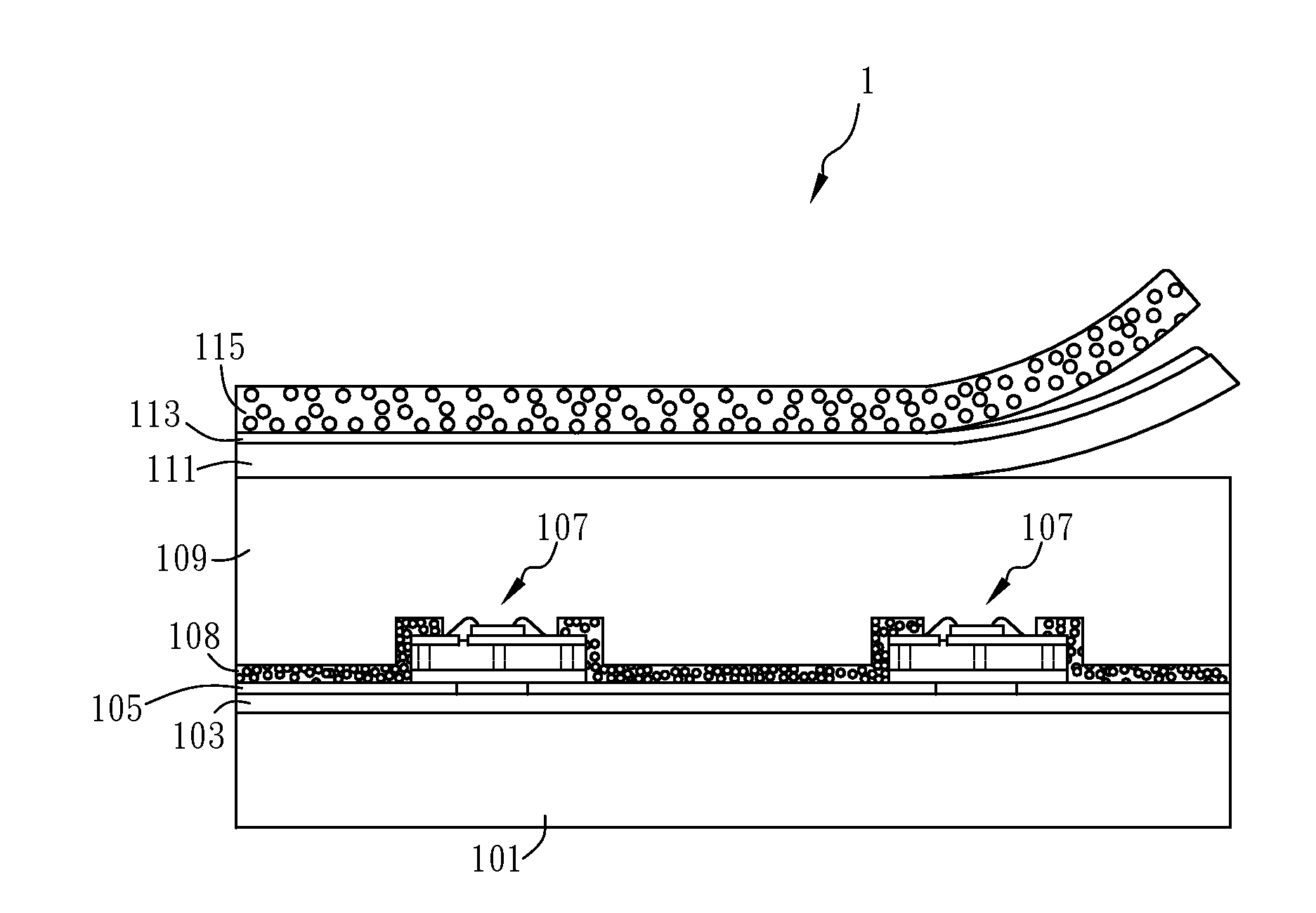
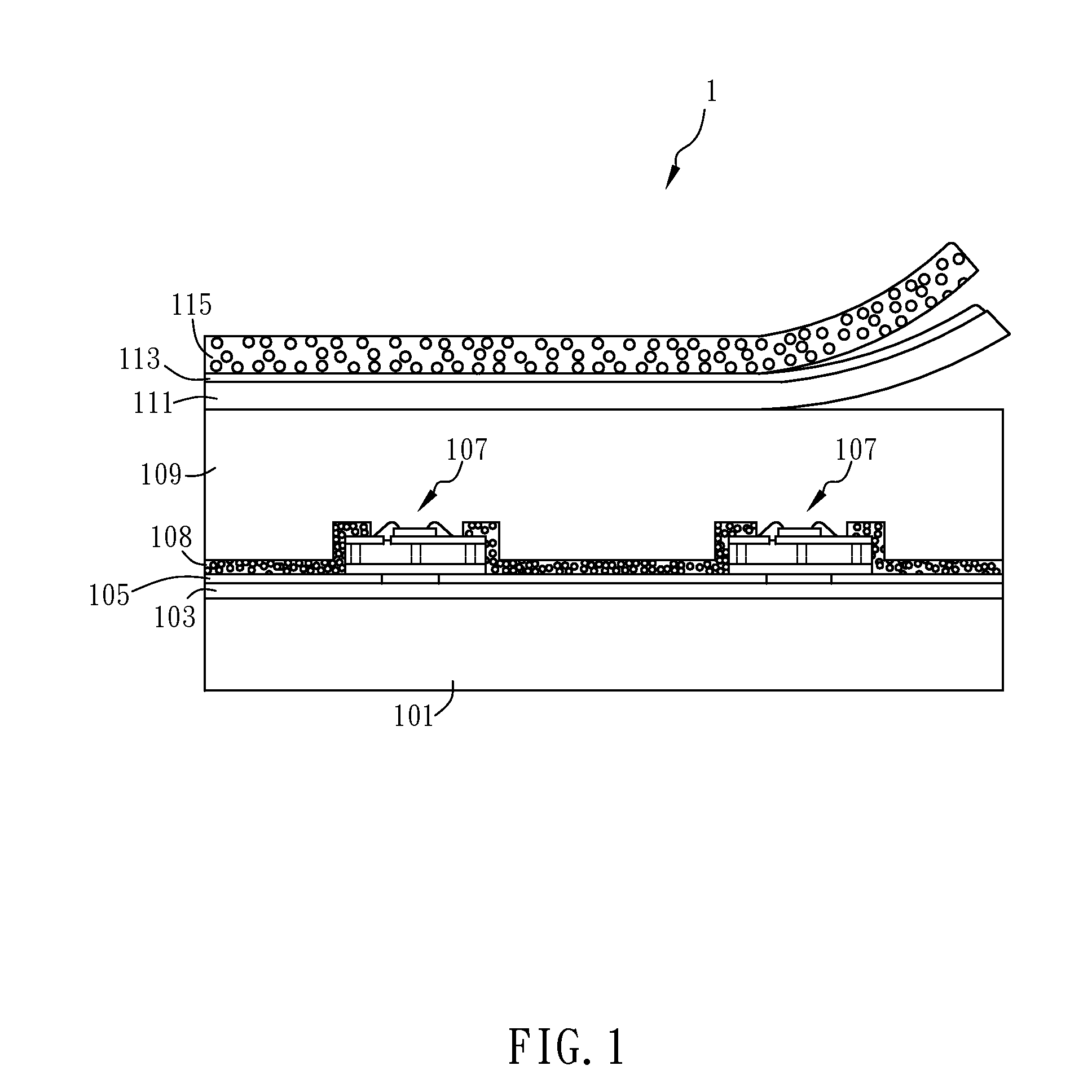
[0033]The present invention relates to a lighting device, for example, a direct-type backlight module. FIG. 1 shows the lighting device 1 in accordance with the present invention. The lighting device 1 at least comprises a substrate 101, an electrode layer 105 patterned on the substrate 101, and a plurality of light source units 107. The light source units 107 are arranged onto the substrate to electrically connect with the electrode layer 105. In this embodiment, it is characterized in that each light source unit 107 includes a circuit board unit and at least one light emitting diode (LED) die being packaged onto the circuit board unit. Certainly, the lighting device 1 further comprises a control circuit (not shown in the figures) electrically connects with the electrode layer 105. The control circuit is capable of selectively activating the plurality of light source units 107 through the electrode layer 105 according to the displayed image to achieve the objective of local dimming...
fourth embodiment
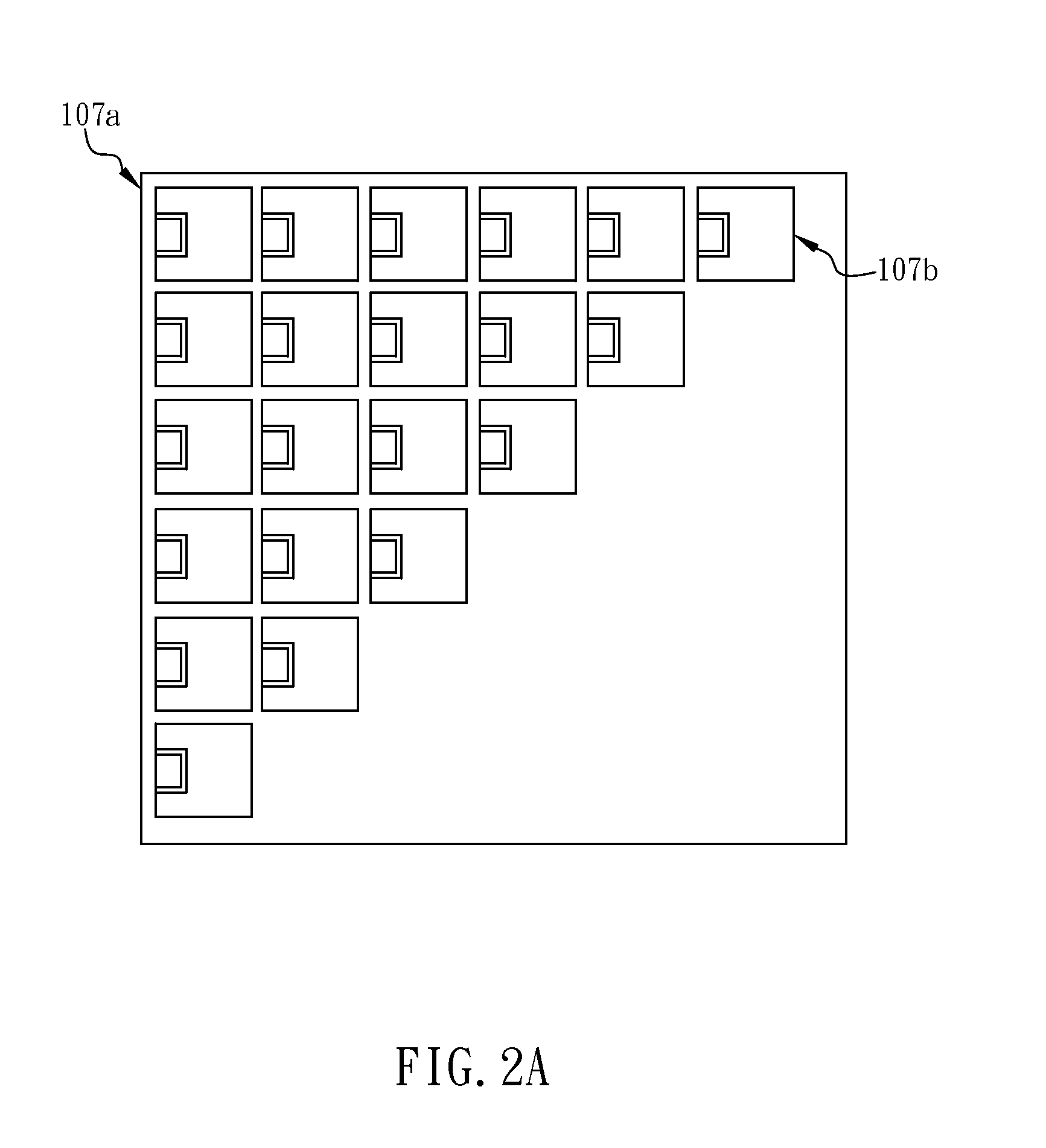
[0050]It is noted that the number of LED dice packaged onto the light source unit 107 is not limited. FIG. 13A to FIG. 13C illustrate the present invention. In this embodiment, a plurality of LED dice 107e are bonded onto one circuit board unit 107b to form one light source unit 107. The metal layers 107c are purposely designed for electrically connecting with the patterned electrode layer 105, as shown in FIG. 13B. The patterned electrode layer 105 is also designed to create X-Y passive matrix driving. Thus, the LED dice 107e can be independently controlled via the electrode layer 105. Certainly, a plurality of light source units 107 can be further assembled onto the substrate 101 and connected with the electrode layer 105, as shown in FIG. 13C. Alternatively, as shown in FIGS. 13D to 13F, the electrical connection between the light source units 107 and the electrode layer 105 can also be formed by creating holes or recesses on the substrate 101, where the size and shape of the hol...
fifth embodiment
[0051]The fifth embodiment discloses a lighting device 1 formed with partitions between the light source units 107. As shown in FIG. 14A and FIG. 14B, a plurality of isolation grid structures 121 is formed within the transparent layer 109 to partition the plurality of light source units 107. The isolation grid structures 121 can be formed by screen printing, inkjet printing, stamping, or any other direct pattern-printing processes in advance and the transparent layer 109 be coated subsequently. Alternatively, the transparent layer 109 can be formed in advance and the isolation grid structures 121 being planted into the transparent layer 109 which can be made by any conventional molding process or knife punching method. It is noted that the materials of isolation grid structures 121 is not limited and is preferred to be white and non-transparent or semi-transparent, so as to block the light from the adjacent the light source units 107. The lighting device 1 of this embodiment is to p...
PUM
 Abstract
Description
Claims
Application Information