Fingerprint identification chip packaging structure and packaging method thereof

A chip packaging structure and fingerprint recognition technology, applied in character and pattern recognition, instruments, electrical components, etc., can solve the problems of low yield, difficult to reduce packaging thickness, and high chip design requirements, and achieve simple connection and wiring process. The effect of package thickness

Active Publication Date: 2016-10-05
深圳明阳芯蕊半导体有限公司
View PDF6 Cites 11 Cited by
  • Summary
  • Abstract
  • Description
  • Claims
  • Application Information

AI Technical Summary

Problems solved by technology

The existing fingerprint identification chip packaging process is complex and difficult (especially the trench corrosion process, the glue overflow control of the sealing process), which requires high chip design, low yield rate, and it is difficult to reduce the overall package thickness.

Method used


Image

  • Fingerprint identification chip packaging structure and packaging method thereof
  • Fingerprint identification chip packaging structure and packaging method thereof
  • Fingerprint identification chip packaging structure and packaging method thereof

Examples


Embodiment Construction

[0037] The present invention will be further described in detail below in conjunction with the accompanying drawings and specific embodiments.

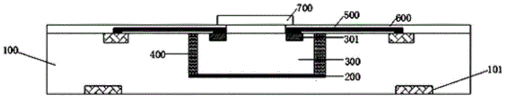
[0038] An embodiment of the present invention, such as figure 2 As shown, a fingerprint identification chip packaging structure, including:

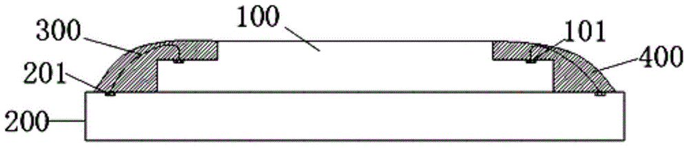
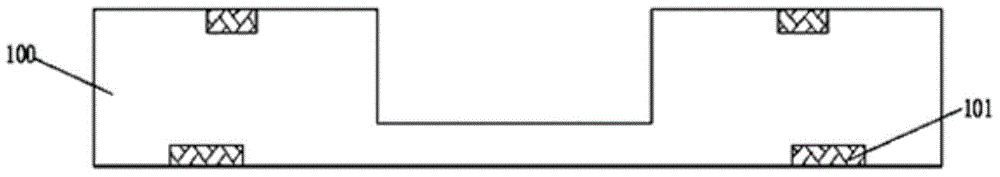
[0039] A substrate 100, the substrate 100 is provided with grooves;

[0040] A chip 300 for fingerprint identification is embedded in the groove.

[0041] Embedding the chip 300 in the groove processed on the substrate 100 can effectively reduce the thickness of the package. Since the upper surface of the chip 300 is basically flush with the upper surface of the substrate 100, the connection and wiring process between the electrodes is very simple. , so it can well solve the problems existing in the prior art.

[0042] Generally speaking, in order to facilitate installation and prevent damage to the chip 300 during installation, the size of the groove should be larger than the size of the ch...


PUM


Abstract

The invention discloses a fingerprint recognition chip packaging structure, comprising: a substrate, the substrate is provided with a groove or a hollow part penetrating through the substrate; a chip for fingerprint recognition is embedded in the groove or the hollow part middle. Embedding the chip in the groove or hollow part processed on the substrate can effectively reduce the thickness of the package. Since the upper surface of the chip is basically flush with the upper surface of the substrate, the connection and wiring process between the electrodes is very simple. Therefore, the problems existing in the prior art can be well solved.

Description

technical field [0001] The invention relates to a chip packaging structure, in particular to a fingerprint identification chip packaging structure and a packaging method thereof. Background technique [0002] In recent years, with the advancement of society and the development of technology, e-commerce services such as mobile wallets, mobile banking, and online shopping have become more and more widely used on smart mobile devices. The importance of personal identification and personal information security has gradually attracted people's attention. The public has higher and higher requirements for the performance of integrated electronic components and network information security. As a kind of biometric identification technology, fingerprint identification is more and more widely used due to its remarkable advantages in safety and convenience. [0003] Especially for mobile terminals, such as mobile phones, notebook computers, tablet computers, digital cameras, etc., the...

Claims


Application Information

Patent Timeline
Patent Type & Authority Applications(China)
IPC IPC(8): H01L23/31H01L21/50H01L21/56H01L23/48G06K9/00
CPCH01L21/568H01L2224/04105H01L2224/19H01L2924/15153H01L2924/18162
Inventor 吴勇军曹凯
Owner 深圳明阳芯蕊半导体有限公司
Why Eureka
Try Eureka