Package carrier and manufacturing method thereof

a packaging and manufacturing method technology, applied in the field of packaging structure, can solve the problem of difficult to significantly reduce and achieve the effect of reducing the thickness of the package structure using the package carrier

Active Publication Date: 2015-04-02
SUBTRON TECH
View PDF4 Cites 11 Cited by
  • Summary
  • Abstract
  • Description
  • Claims
  • Application Information

AI Technical Summary

Benefits of technology

[0005]The present invention is directed to a package carrier capable of carrying a chip and the thickness of a package structure using the package carrier is reduced.
[0009]In light of the foregoing descriptions, the manufacturing processes of the package carrier in the invention are symmetrically performed on two base metal layers bonded with each other. Therefore, two independent package carriers are formed simultaneously after the base metal layers are separated, so as to save the manufacturing time and improve the production efficiency. In addition, the package carrier of the invention adopts the patterned metal layer to carry and electrically connects the chip, and the release metal film is connected between the supporting layer and the patterned metal layer, such that the supporting layer can be easily removed after the molding process by adopting the separable characteristic of the release metal film. Therefore, comparing with the conventional package carrier composed of a plurality of patterned circuit layers and patterned dielectric layers alternately stacked on the core dielectric layer, the package carrier of the invention allows the package structure using said package carrier to have a thinner overall thickness.

Problems solved by technology

Therefore, if there is a bottleneck in reducing the thickness of the core dielectric layer, it will be hard for the whole thickness of the package structure to be remarkably reduced.

Method used


Image

  • Package carrier and manufacturing method thereof
  • Package carrier and manufacturing method thereof
  • Package carrier and manufacturing method thereof

Examples


Embodiment Construction

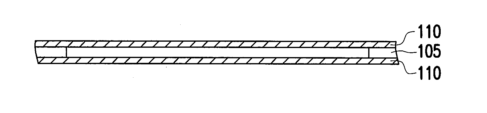
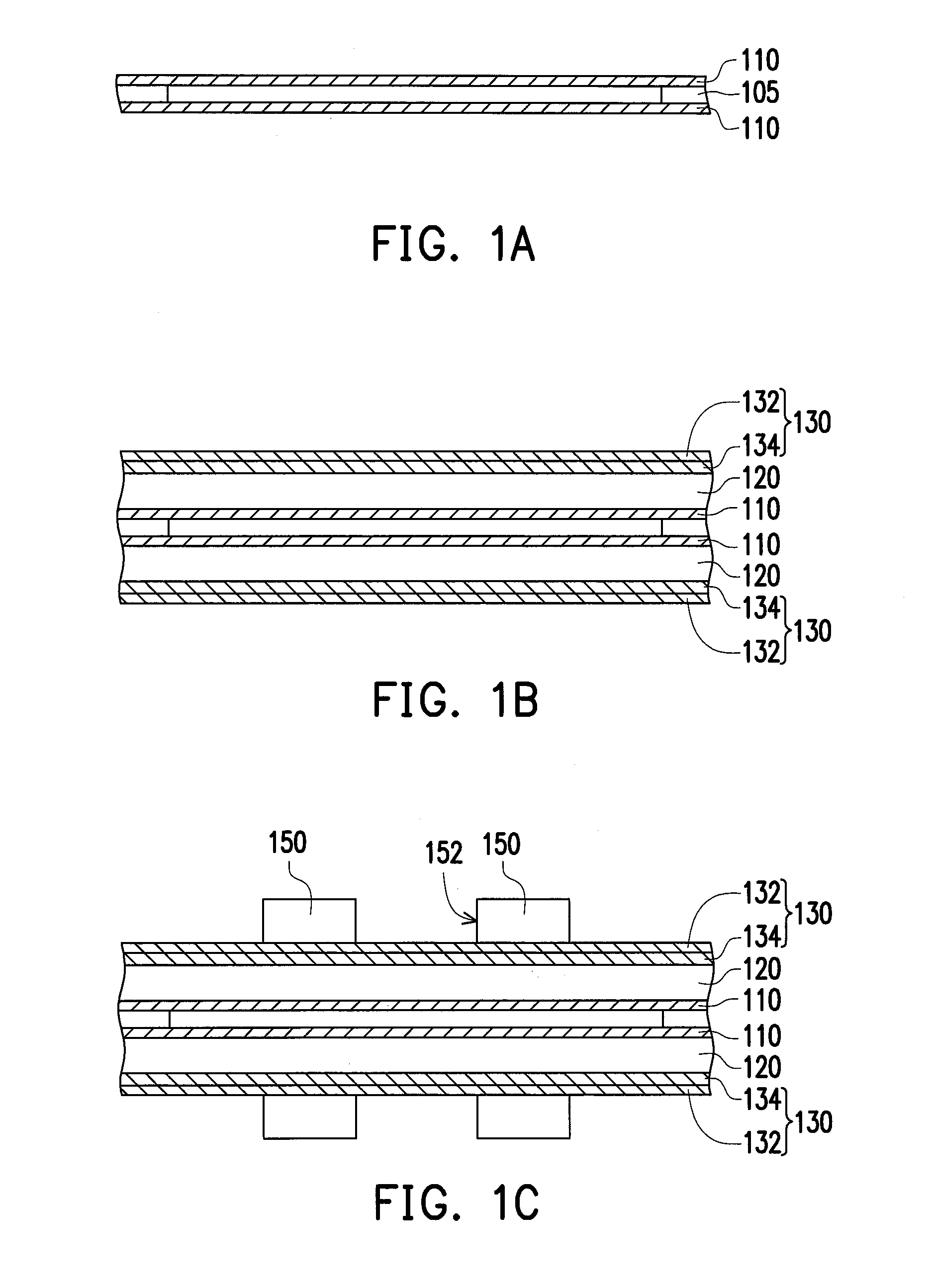
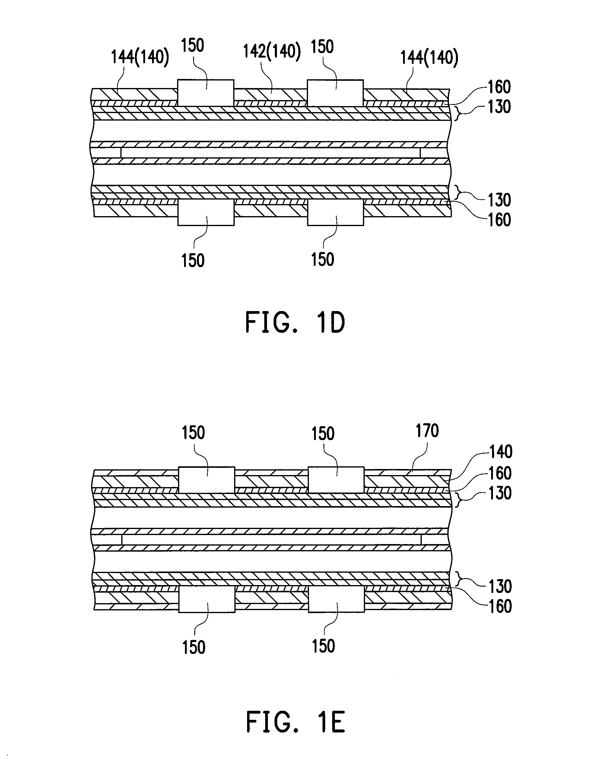
[0013]FIGS. 1A to 1G are schematic cross-sectional views illustrating manufacturing steps of a package carrier according to an embodiment of the present invention. In the present embodiment, a manufacturing method of a package carrier includes the following steps. Firstly, referring to FIG. 1A, two base metal layers 110 are bonded. In the present embodiment, the two base metal layers 110 may be two copper foils, and is bonded by dispensing an adhesive layer 105 on edges of the two base metal layers 110 to form a sealing region at the edges of the two base metal layers 110, such that the two base metal layers can be bonded together temporarily for preventing infiltration of chemicals or reagents used in subsequent processes.

[0014]Referring to FIG. 1B, two supporting layers 120 are laminated onto the base metal layers 110 respectively. Then, two release metal films 130 are disposed on the supporting layers 120 respectively, wherein each of the release metal films 130 includes a first ...


PUM

PropertyMeasurementUnit
thicknessaaaaaaaaaa
thicknessaaaaaaaaaa
widthaaaaaaaaaa

Abstract

A manufacturing method of a package carrier includes the following steps. Firstly, two base metal layers are bonded together. Then, two supporting layers are laminated onto the base metal layers respectively. Next, two release metal films are disposed on the supporting layers respectively, wherein each of the release metal films includes a first metal film and a second metal film separable from each other. Next, two patterned metal layers are formed on the release metal films respectively, wherein each of the patterned metal layers is suitable for carrying and electrically connected to a chip. Then, the base metal layers are separated from each other to form two package carriers independent from each other. A package carrier formed by the manufacturing method described above is also provided.

Description

CROSS-REFERENCE TO RELATED APPLICATION[0001]This application claims the priority benefit of Taiwan application serial no. 102135030, filed on Sep. 27, 2013. The entirety of the above-mentioned patent application is hereby incorporated by reference herein and made a part of this specification.BACKGROUND OF THE INVENTION[0002]The present invention relates to a package structure and a manufacturing method thereof. More particularly, the present invention relates to a package carrier and a manufacturing method thereof.DESCRIPTION OF RELATED ART[0003]The purpose of chip packages is to protect exposed chips, to reduce contact density in a chip, and to provide good thermal dissipation for chips. The chip can be connected to the carrier by wire bonding or by flip chip bonding, such that the bonding pads on the chip can be electrically connected to contacts of the carrier, thereby forming a chip package. Therefore, the contacts on the chip can be re-distributed through the package carrier, s...

Claims


Application Information

Patent Timeline
Patent Type & Authority Applications(United States)
IPC IPC(8): H01L23/00H05K1/09H05K13/04H05K1/11
CPCH01L24/85H05K13/046H05K1/09H05K1/111H01L21/4825H01L21/4832H01L21/568H01L21/6835H01L23/3128H01L23/49541H01L23/49582H01L24/16H01L24/29H01L24/32H01L24/48H01L24/81H01L24/83H01L2221/68345H01L2221/68359H01L2224/16245H01L2224/2919H01L2224/32245H01L2224/48091H01L2224/48105H01L2224/48245H01L2224/81005H01L2224/81439H01L2224/81444H01L2224/81447H01L2224/8149H01L2224/83005H01L2224/83439H01L2224/83444H01L2224/83447H01L2224/8349H01L2224/85H01L2224/85005H01L2224/85439H01L2224/85444H01L2224/85447H01L2224/8549H01L2924/00014H01L2924/15311H01L2924/181H01L2924/3511H01L2224/45099H01L2924/00012H01L2924/00
Inventor SUN, SHIH-HAO
Owner SUBTRON TECH
Why Eureka
Try Eureka