Electronic package and manufacturing method thereof

a technology of electronic packaging and manufacturing methods, applied in the direction of electrical apparatus, semiconductor devices, semiconductor/solid-state device details, etc., can solve the problem of thicker chip packaging, and achieve the effect of reducing the size of the chip

Active Publication Date: 2018-01-11
HU DYI CHUNG
View PDF13 Cites 11 Cited by
  • Summary
  • Abstract
  • Description
  • Claims
  • Application Information

AI Technical Summary

Benefits of technology

[0005]The invention provides an electronic package and a manufacturing method thereof, which effectively reduces the size thereof.

Problems solved by technology

The disadvantage for such chip package is that it uses a rigid interposer which makes the chip package thicker.

Method used


Image

  • Electronic package and manufacturing method thereof
  • Electronic package and manufacturing method thereof
  • Electronic package and manufacturing method thereof

Examples


Embodiment Construction

[0013]Reference will now be made in detail to the present preferred embodiments of the invention, examples of which are illustrated in the accompanying drawings. Wherever possible, the same reference numbers are used in the drawings and the description to refer to the same or like parts.

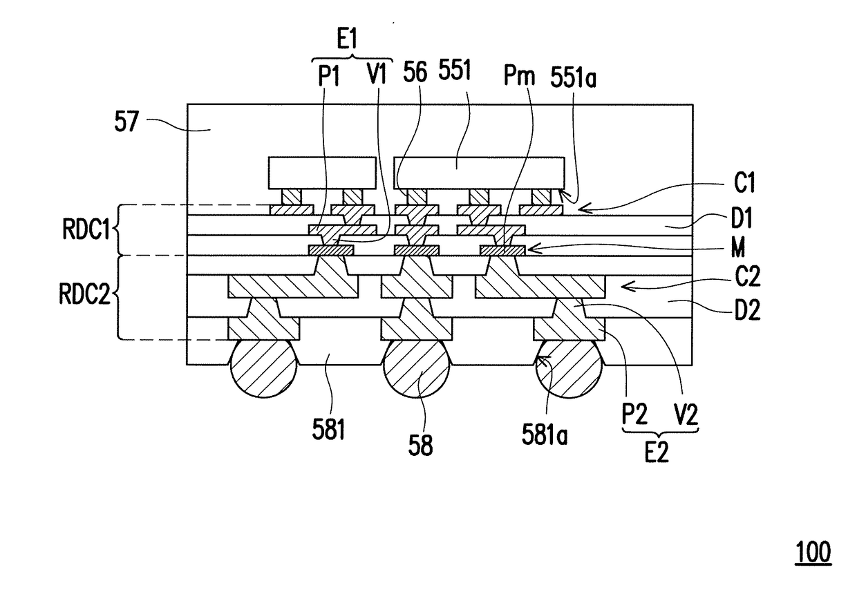
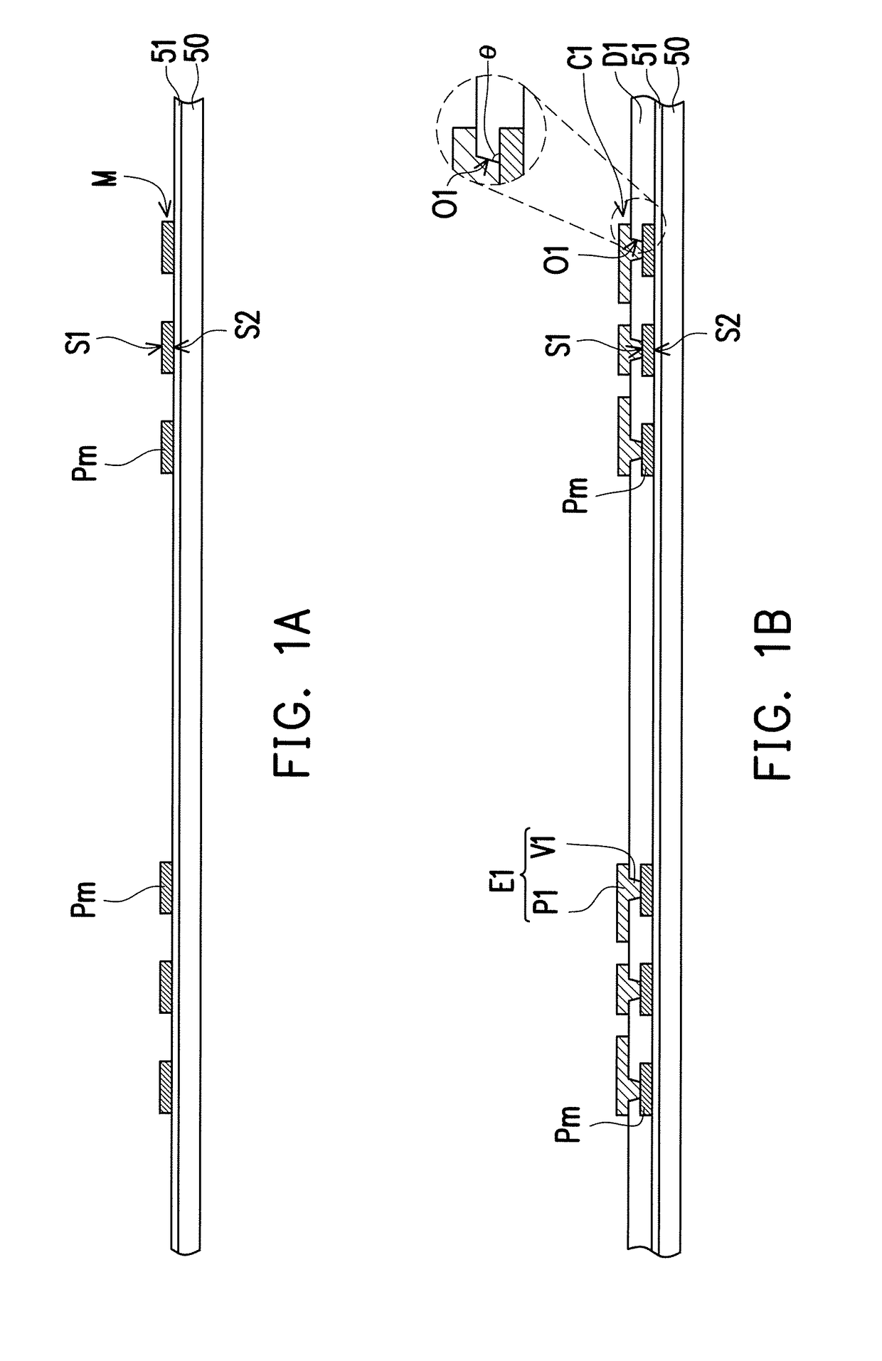
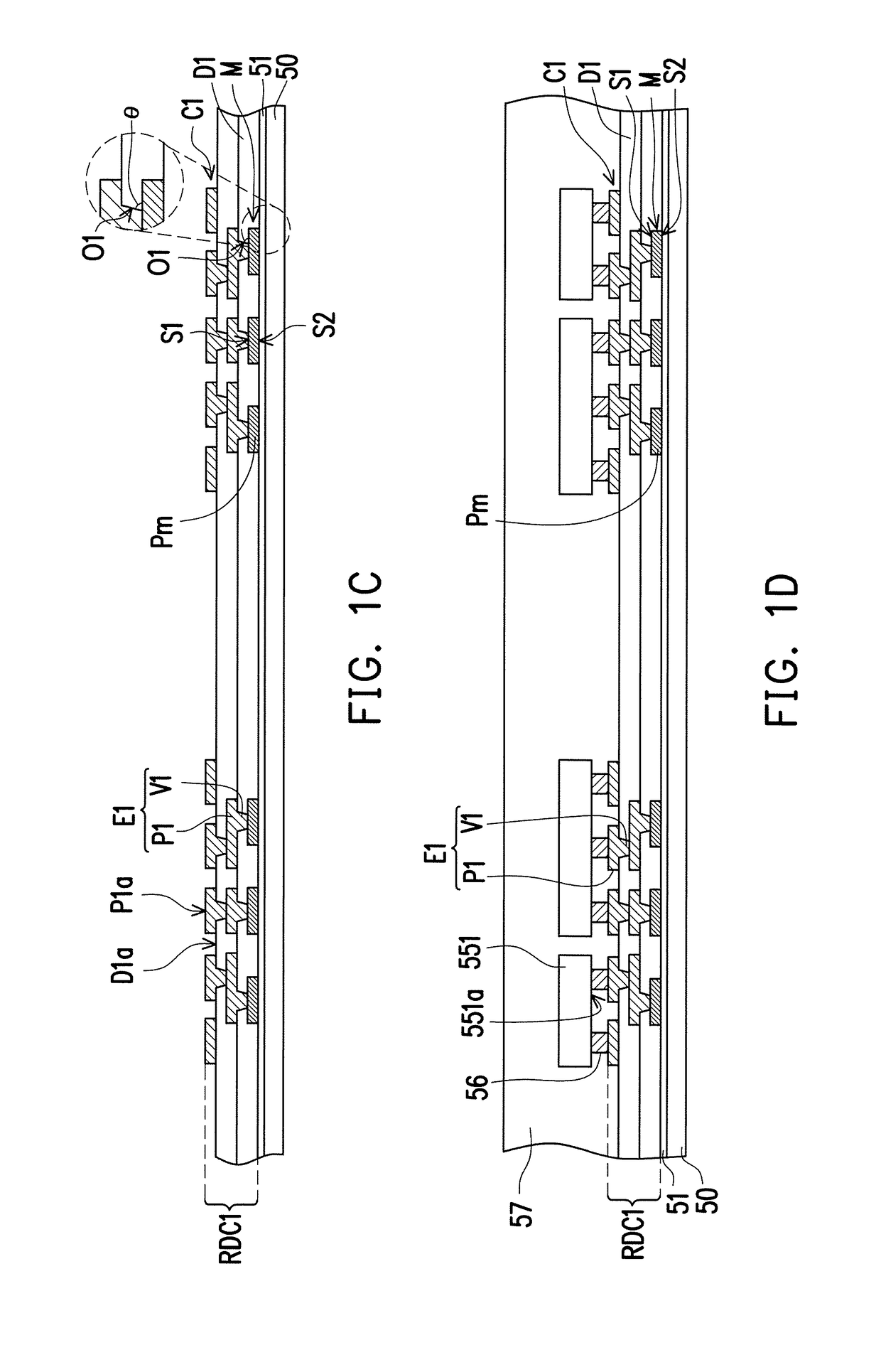
[0014]FIG. 1A to FIG. 1I are schematic cross-sectional views illustrating a manufacturing method of an electronic package according to an embodiment of the invention.

[0015]Referring to FIG. 1A, a middle patterned conductive layer M is formed on a temporary carrier 50. For example, the middle patterned conductive layer M has a first surface S1, a second surface S2 opposite to the first surface and facing towards the temporary carrier 50 and a plurality of middle conductive pads Pm. In some embodiments, a release layer 51 is applied on a top surface of a temporary carrier 50 to enhance the releasability of the middle patterned conductive layer M from the temporary carrier 50 in the subsequent process. ...


PUM


Abstract

An electronic package including a middle patterned conductive layer, a first redistribution circuitry disposed on a first surface of the middle patterned conductive layer and a second redistribution circuitry disposed on a second surface of the middle patterned conductive layer is provided. The middle patterned conductive layer has a plurality of middle conductive pads. The first redistribution circuitry includes a first patterned conductive layer having a plurality of first conductive elements. Each of the first conductive elements has a first conductive pad and a first conductive via that form a T-shaped section. The second redistribution circuitry includes a second patterned conductive layer having a plurality of second conductive elements. Each of the second conductive elements has a second conductive pad and a second conductive via that form an inversed T-shaped section.

Description

CROSS REFERENCE TO RELATED APPLICATION[0001]This application claims the priority benefit of U.S. provisional application Ser. No. 62 / 359,755, filed on Jul. 8, 2016. The entirety of the above-mentioned patent application is hereby incorporated by reference herein and made a part of specification.BACKGROUND OF THE INVENTION1. Field of the Invention[0002]The present invention relates to a package structure, especially relates to an electronic package without having any interposer therein.2. Description of Related Art[0003]Conventionally, taking U.S. patent publication number 2014 / 0102777 for example, a chip package uses a rigid interposer as a package support. For example, a semiconductor chip is mounted onto the top electrode pads of the top redistribution layer through conductive bumps, and a solder ball can be disposed on each of the bottom conductive pads of the circuit built-up structure configured on bottom of the interposer. A molding layer is formed to encapsulate the interpose...

Claims


Application Information

Patent Timeline
Patent Type & Authority Applications(United States)
IPC IPC(8): H01L21/48H01L21/56H01L21/683H01L25/065H01L23/498H01L23/00H01L25/00
CPCH01L21/4853H01L2224/16227H01L21/481H01L21/568H01L21/561H01L21/6835H01L23/49816H01L23/49838H01L23/49822H01L24/97H01L24/16H01L25/0655H01L25/50H01L2221/68345H01L2221/68359H01L2224/95001H01L21/4857H01L23/3128H01L2224/81005H01L2224/97H01L2924/15311H01L2924/18161H01L23/5383H01L2924/181H01L24/13H01L24/32H01L24/73H01L24/81H01L2224/13147H01L2224/16225H01L2224/32225H01L2224/73204H01L2224/92125H01L2224/81H01L2924/00012H01L2924/00014H01L2924/00
Inventor HU, DYI-CHUNG
Owner HU DYI CHUNG
Why Eureka
Try Eureka