Semiconductor package and fabrication method thereof

a technology of semiconductors and packaging, applied in the direction of semiconductor devices, semiconductor/solid-state device details, electrical apparatus, etc., can solve the problems of limiting the i/o density of the overall package structure, the height of the pop structure as well as the thickness of an electronic device having the pop structure cannot be effectively reduced, and the chips on the packaging substrate and the interconnection structure are susceptible to moisture intrusion, so as to reduce the thickness of the package and save the surface area of the packaging substrate. ,

Active Publication Date: 2015-07-02
SILICONWARE PRECISION IND CO LTD
View PDF3 Cites 12 Cited by
  • Summary
  • Abstract
  • Description
  • Claims
  • Application Information

AI Technical Summary

Benefits of technology

[0012]The semiconductor package of the present invention uses the conductive posts instead of the conventional solder balls as an interconnection structure for a PoP structure and the upper surfaces of the encapsulant and the conductive posts are flush with the inactive surface of the chip, thereby increasing the package density, reducing the package thickness and saving the surface area of the packaging substrate. Further, the encapsulant formed between the lower packaging substrate and an upper electronic element protects the chip and the interconnection structure from being adversely affected by intrusion of moisture.

Problems solved by technology

As such, the interconnection structure occupies a large area of the packaging substrate and limits the I / O density of the overall package structure.
Further, since the solder ball interconnection structure must be higher than chips on the substrate, the height of the PoP structure as well as the thickness of an electronic device having the PoP structure cannot be effectively reduced.
Furthermore, since no encapsulant is formed between the lower packaging substrate and the upper electronic element, the chips on the packaging substrate and the interconnection structure are susceptible to intrusion of moisture.

Method used


Image

  • Semiconductor package and fabrication method thereof
  • Semiconductor package and fabrication method thereof
  • Semiconductor package and fabrication method thereof

Examples


Embodiment Construction

[0016]The following illustrative embodiments are provided to illustrate the disclosure of the present invention, these and other advantages and effects can be apparent to those in the art after reading this specification.

[0017]It should be noted that all the drawings are not intended to limit the present invention. Various modifications and variations can be made without departing from the spirit of the present invention.

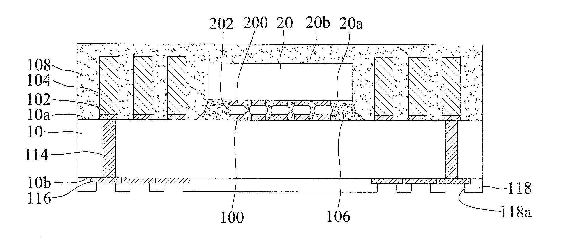
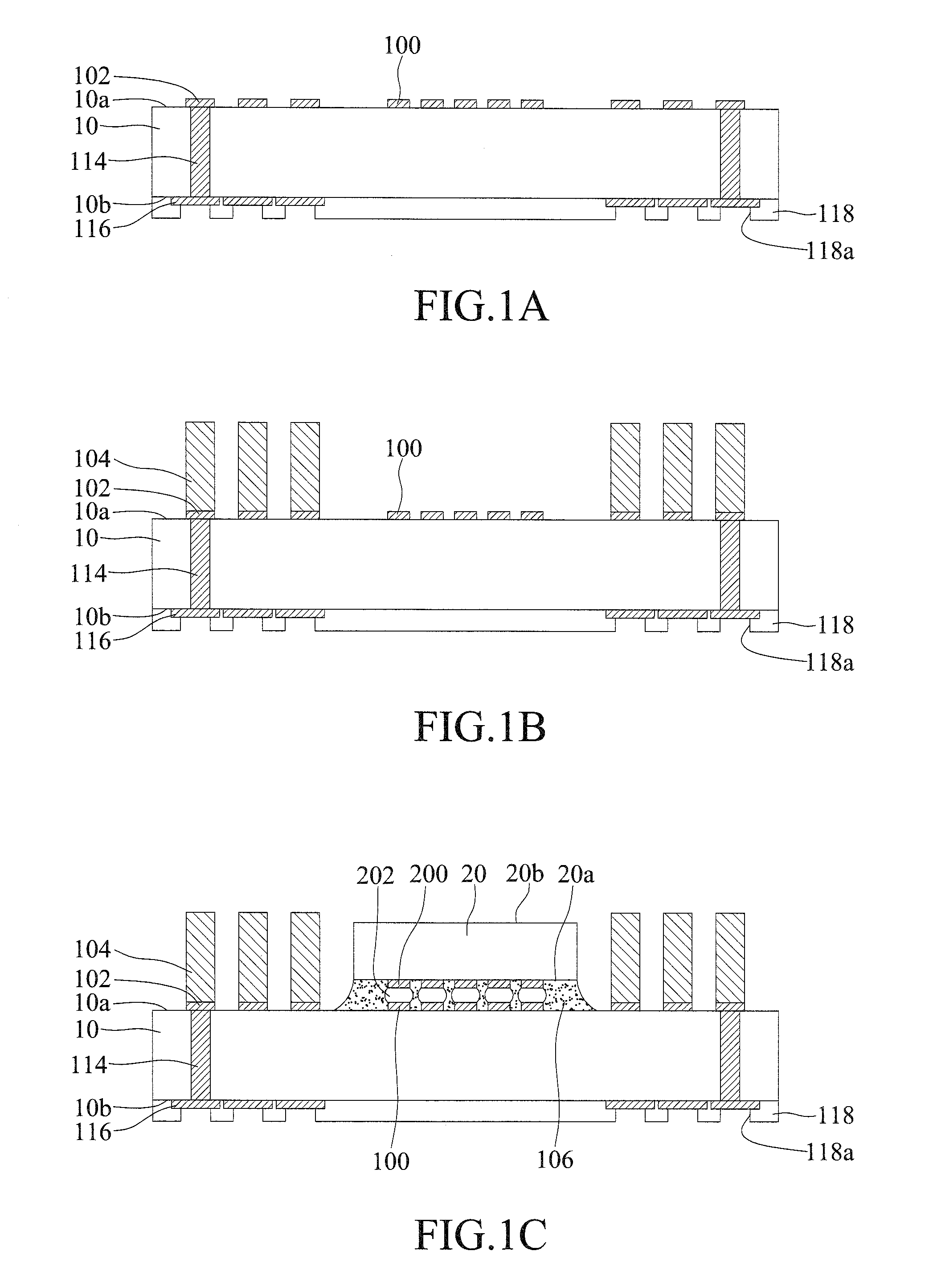
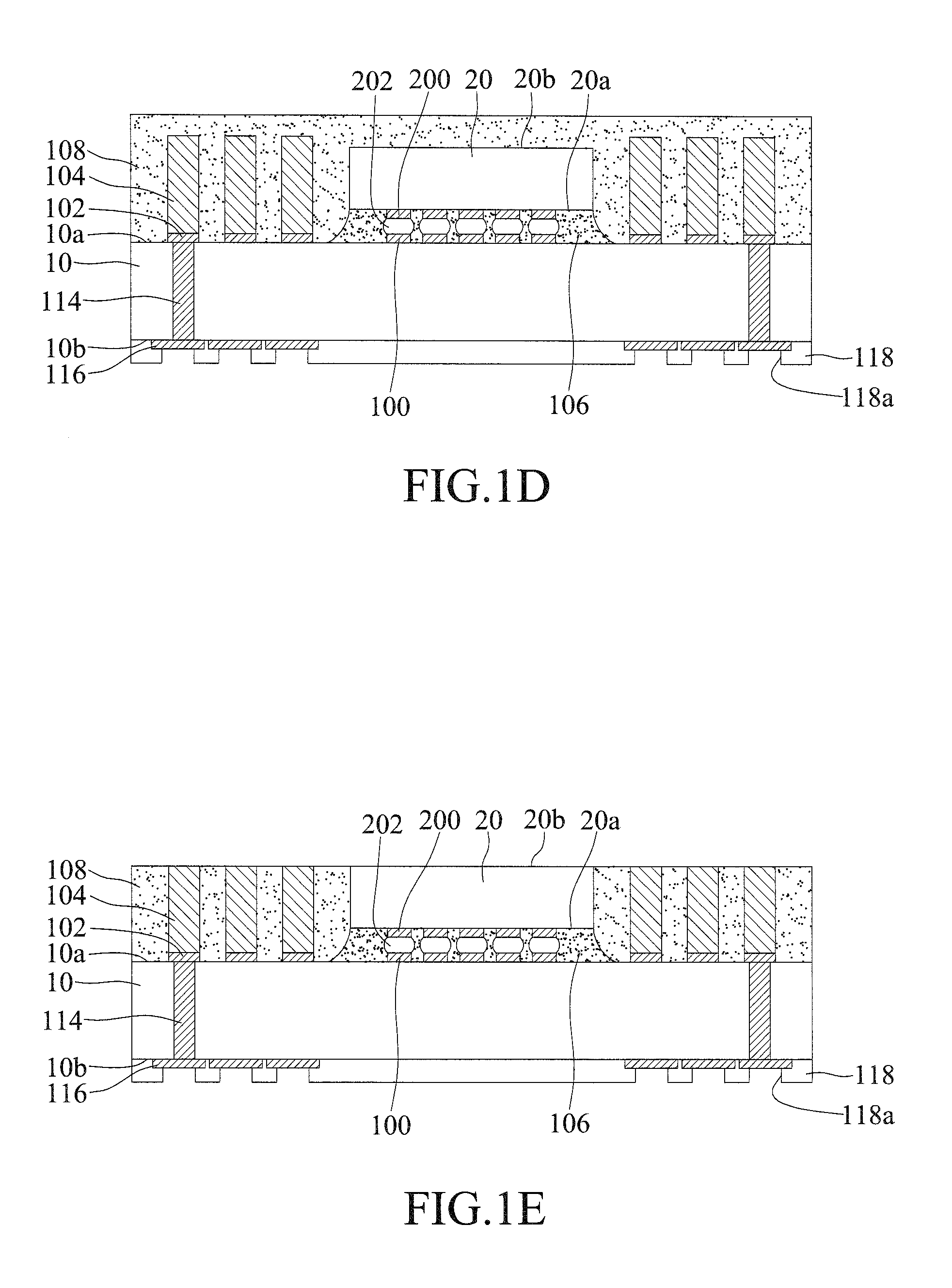
[0018]FIGS. 1A to 1G are schematic cross-sectional views showing a method for fabricating a semiconductor package according to the present invention.

[0019]Referring to FIG. 1A, a packaging substrate 10 is provided. The package substrate 10 has opposite first and second surfaces 10a, 10b and a plurality of first and second conductive pads 100, 102 formed on the first surface 10a. Further, the packaging substrate 10 can have a plurality of third conductive pads 116 formed on the second surface 10b of the packaging substrate 10 and a plurality of conductive through hol...


PUM


Abstract

A semiconductor package is provided, which includes: a packaging substrate having opposite first and second surfaces and a plurality of first and second conductive pads formed on the first surface; a chip having opposite active and inactive surfaces and disposed on the first conductive pads via the active surface thereof; a plurality of conductive posts formed on the second conductive pads, respectively; and a first encapsulant formed on the first surface of the packaging substrate for encapsulating the chip and the conductive posts and having a plurality of openings for exposing upper surfaces of the conductive posts, thereby increasing the package density and protecting the chip and the interconnection structure from being adversely affected by intrusion of moisture.

Description

BACKGROUND OF THE INVENTION[0001]1. Field of the Invention[0002]The present invention relates to semiconductor packages and fabrication methods thereof, and more particularly, to a semiconductor package having conductive posts and a fabrication method thereof.[0003]2. Description of Related Art[0004]In recent years, package on package (PoP) structures have become a focus since they meet the miniaturization requirement of electronic products by saving surface area of substrates and at the same time have an improved processing performance.[0005]In a conventional PoP structure, solder balls serve as an interconnection structure for electrically connecting a lower packaging substrate and an upper electronic element. However, to prevent solder bridging during a reflow process, the pitch between the solder balls must be greater than 300 um. As such, the interconnection structure occupies a large area of the packaging substrate and limits the I / O density of the overall package structure.[0...

Claims


Application Information

Patent Timeline
Patent Type & Authority Applications(United States)
IPC IPC(8): H01L23/00H01L23/31H01L21/56
CPCH01L24/17H01L2924/14H01L24/81H01L21/563H01L23/3142H01L2224/13147H01L2224/16057H01L2224/13023H01L2224/16147H01L2224/16227H01L2224/17151H01L2224/1183H01L2224/81801H01L2224/8136H01L24/11H01L23/3128H01L23/3135H01L2224/16225H01L24/16H01L2224/05647H01L2224/16237H01L2224/16238H01L2224/32225H01L2224/73204H01L2224/81815H01L2224/92125H01L2924/18161H01L2224/05568H01L2224/0401H01L2224/131H01L23/49816H01L21/4853H01L23/5389H01L23/49811H01L2924/00014H01L2924/00H01L2924/014H01L21/486
Inventor CHIANG, CHENG-CHIAJIANG, DON-SONWANG, LUNG-YUANTUNG, SHIH-HAOHUANG, SHU-HUEI
Owner SILICONWARE PRECISION IND CO LTD
Why Eureka
Try Eureka