High density memory card assembly

a memory card and high density technology, applied in the direction of printed circuit parts, printed circuit non-printed electric components association, instruments, etc., can solve the problems of more complicated package assembly procedure than that used, stacked-die package having a single defective ic device becoming completely unusable, and increasing the overall height or area consumed, so as to increase the density of memory card and increase the overall height or area. consumption, the effect of increasing the density of the memory card

Active Publication Date: 2008-01-08
KINGSTON DIGITAL CO LTD
View PDF19 Cites 95 Cited by
  • Summary
  • Abstract
  • Description
  • Claims
  • Application Information

AI Technical Summary

Benefits of technology

[0009]In general terms, what is disclosed herein is a digital storage memory card such as a USB drive, SD card, MMC card, or a CF card having one or more flash memory device packages to provide non-volatile, digital memory storage. More particularly, a high density arrangement is provided for a memory card assembly using a leadframe type package, such as TSOP, on one or both sides of a flex or rigid-flex substrate to increase the memory package density without substantially increasing the overall height or area consumed. By virtue of the foregoing, the assembly can comfortably fit inside an external housing that has been allocated for typical USB drives and other card formats.

Problems solved by technology

However, such a stacked-die package is more difficult and expensive to manufacture.
In addition, the package assembly procedure is more complicated than that used for a standard, single-die package assembly.
In other cases, the stacked-die package having a single defective IC device may become entirely unusable.
Consequently, if the test yield is low, it can prove to be costly in situations where stacked-die packages are used to achieve high density for memory cards.

Method used


Image

  • High density memory card assembly
  • High density memory card assembly
  • High density memory card assembly

Examples


Embodiment Construction

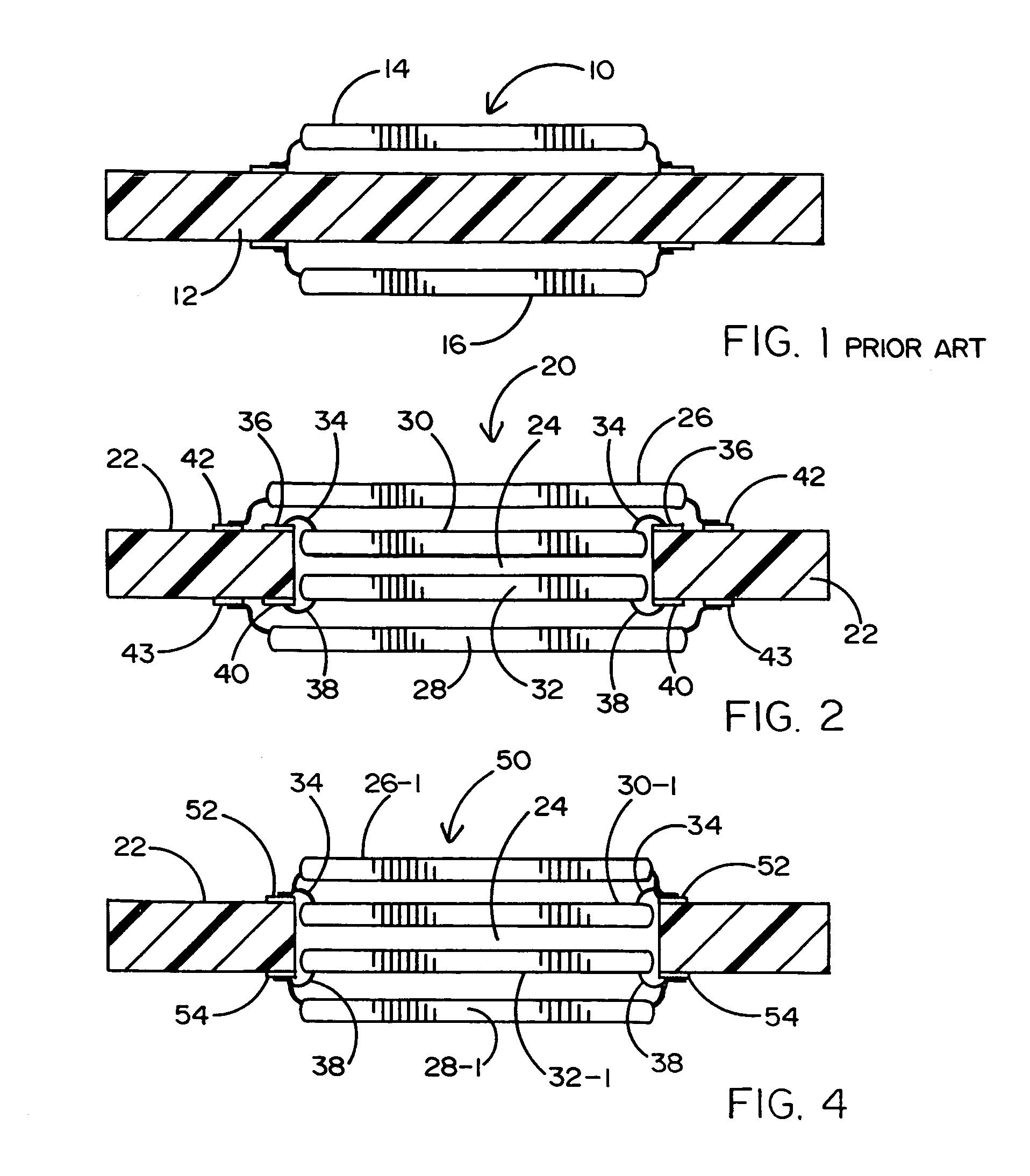
[0015]Turning now to the drawings, FIG. 1 shows a conventional memory card 10 having a rigid, solid laminate substrate 12. A first leadframe memory package 14 is connected to one side of the substrate 12, and a second leadframe memory package 16 is connected to the opposite side of the substrate 12. The overall height of the memory card 10 of FIG. 1 must be sufficiently low to fit within an external housing. By way of example, for an MMC card, the overall thickness is limited to 1.4 mm. In the conventional case, the storage capacity of memory card 10 is limited to the leadframe memory packages 14 and 16.

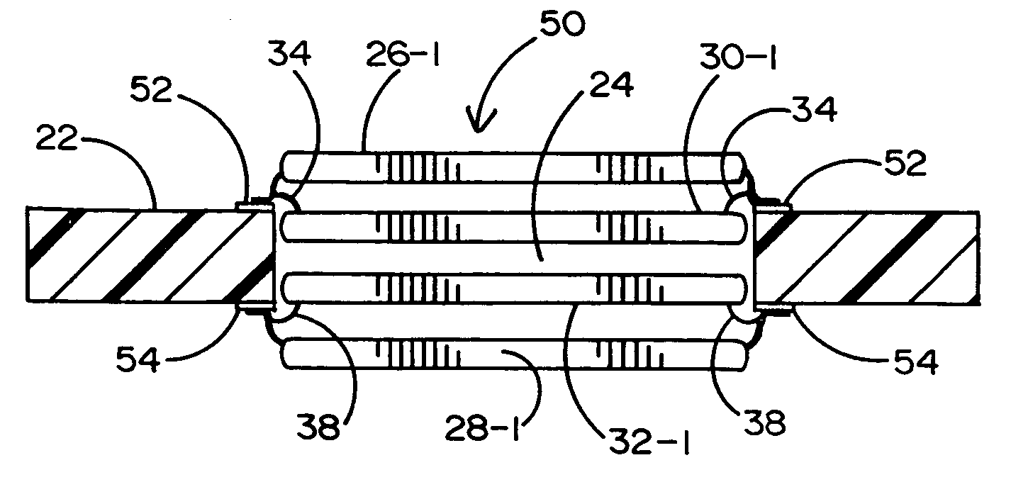
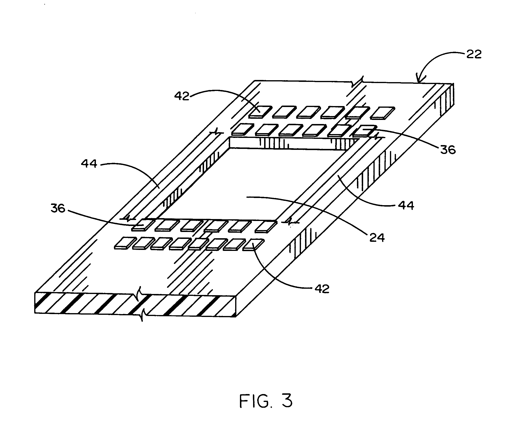
[0016]In accordance with a first preferred embodiment of this invention, a high density memory card assembly 20 having increased non-volatile storage capacity is shown in FIG. 2 of the drawings. The memory card assembly 20 includes either a flex or a rigid-flex substrate 22 having a cavity 24 (best shown in FIG. 3) formed therethrough. Like the conventional memory card 10 of FIG. 1, ...


PUM


Abstract

A high density memory card assembly having application for USB drive storage, flash and ROM memory cards, and similar memory card formats. A cavity is formed through a rigid laminate substrate. First and second digital memory devices (e.g., TSOP packages or bare semiconductor dies) are located within the cavity so as to be recessed relative to the top and bottom of the substrate. The recessed first and second memory devices are arranged in spaced, face-to-face alignment with one another within the cavity. The first and second memory devices are covered and protected by respective first and second memory packages that are located on the top and bottom of the substrate. By virtue of the foregoing, the memory package density of the assembly can be increased without increasing the height or area consumed by the assembly for receipt within an existing external housing.

Description

BACKGROUND OF THE INVENTION[0001]1. Field of the Invention[0002]This invention relates generally to memory device packaging and, more particularly, to high density digital memory cards having application for USB drive storage, flash and ROM memory cards, and other memory cards of similar format.[0003]2. Background Art[0004]Most conventional memory card assemblies (excluding the outside casing) include a rigid laminate substrate, such as an FR-4 printed wiring board (PWB), a controller, the required passive components, and at least one digital (e.g., flash) memory storage device in a TSOP (thin small outline package) type 1 package. The TSOP 1 packages are desirable because of their thin profile, typically only 1.2 mm high, and small overall footprint that can meet the size limitations of a memory card. While a memory card may vary in size and shape, most have limited thickness in order to be able to fit into the slot of a reader that is adapted to receive specific types of memory ca...

Claims


Application Information

Patent Timeline
Patent Type & Authority Patents(United States)
IPC IPC(8): H01L23/34
CPCG11C5/02H01L25/0652H01L25/105H05K1/182H05K2201/10515H05K2201/10545H05K2201/10689H01L2225/1029H01L2225/107H01L2924/0002H01L2924/00
Inventor KOH, WEI H.CHEN, DAVID
Owner KINGSTON DIGITAL CO LTD
Why Eureka
Try Eureka