Semiconductor device and manufacturing method thereof

a technology of semiconductor devices and manufacturing methods, applied in semiconductor devices, semiconductor/solid-state device details, electrical apparatus, etc., can solve the problems of increasing the restricting the use of electrodes, and prone to damage to the bump electrode, so as to reduce the stress caused by the difference between the coefficients of thermal expansion and reduce the stress. , the effect of suppressing the stress

Active Publication Date: 2011-05-17
MICRON TECH INC
View PDF5 Cites 15 Cited by
  • Summary
  • Abstract
  • Description
  • Claims
  • Application Information

AI Technical Summary

Benefits of technology

[0013]The present invention seeks to solve the above problems and provides a semiconductor device capable of suppressing damage to bump electrodes due to stress caused by a difference between coefficients of thermal expansion of a semiconductor chip and a package substrate so as to improve connection reliability, and provides a manufacturing method thereof.
[0015]According to the aspects of the invention, the semiconductor chip is mounted on the package substrate and the dummy chips are mounted on regions close to the four corner portions of the semiconductor chip. Thus, the stress induced to the corner portions of the semiconductor chip is decreased since the dummy chips having a small difference between coefficients of thermal expansion are provided near the corner portions, so that damage to the bump electrodes immediately under the corner portions can be suppressed. Accordingly, the fracture of the bump electrodes can be prevented, thereby improving the connection reliability of the package substrate.
[0017]As described above, according to the present invention, the semiconductor chip and the dummy chips are mounted on one surface of the package substrate, the plurality of bump electrodes are mounted on the other surface of the package substrate, and the difference between the coefficients of thermal expansion can be sufficiently small. Therefore, the stress caused by the difference between the coefficients of thermal expansion can be decreased in regions where the dummy chips are close to the corner portions of the semiconductor chip. Thus, at the bump electrodes under these regions, the damage due to the stress can be suppressed so that the fracture of the bump electrodes can be prevented so as to improve connection reliability of the package substrate. Further, since the mounting of the dummy chips does not affect the arrangement of the plurality of bump electrodes, thereby arranging the bump electrodes in a high density without hindering multi pins and narrow pitch of the semiconductor device.

Problems solved by technology

Such semiconductor devices particularly have a problem of fracture of bump electrodes located in the vicinity of an outer portion of the semiconductor chip among the bump electrodes on the package substrate.
Generally, in the semiconductor chip, a difference between coefficients of thermal expansion is larger than that of the package substrate or resin, and therefore some of the bump electrodes are prone to damage due to stress induced at a boundary portion of the semiconductor chip.
Particularly, since the coefficients of thermal expansion largely differ between a portion where the semiconductor chip exists and a portion where the semiconductor chip does not exist, the damage to the bump electrodes increases in regions close to corner portions of the semiconductor chip relative to other regions.
However, according to the above conventional methods, the effect to prevent the fracture due to the stress concentration on the bump electrodes is restrictive, and is insufficient for improving the connection reliability of the bump electrodes.
That is, the above conventional methods enable to suppress the stress concentration on the bump electrodes in peripheral portions including the corner portions of the package substrate, however it has been discovered that the fracture due to the stress concentration on the bump electrodes is actually prone to occur mainly at the bump electrodes immediately under corner portions of the semiconductor chip, instead of corner portions of the package substrate.
Also, in the above conventional methods, the region where the bump electrodes 101 are not arranged is provided, for example, in a peripheral portion of the package substrate 100, which is a disadvantage in terms of arrangement density of the bump electrodes 101.
Since a semiconductor device having multiple pins and narrow pitch has been strongly demanded, it becomes a problem to solve to implement measures without hindering a high density arrangement of a large number of bump electrodes.

Method used


Image

  • Semiconductor device and manufacturing method thereof
  • Semiconductor device and manufacturing method thereof
  • Semiconductor device and manufacturing method thereof

Examples


first embodiment

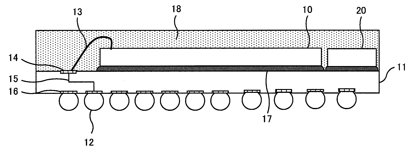
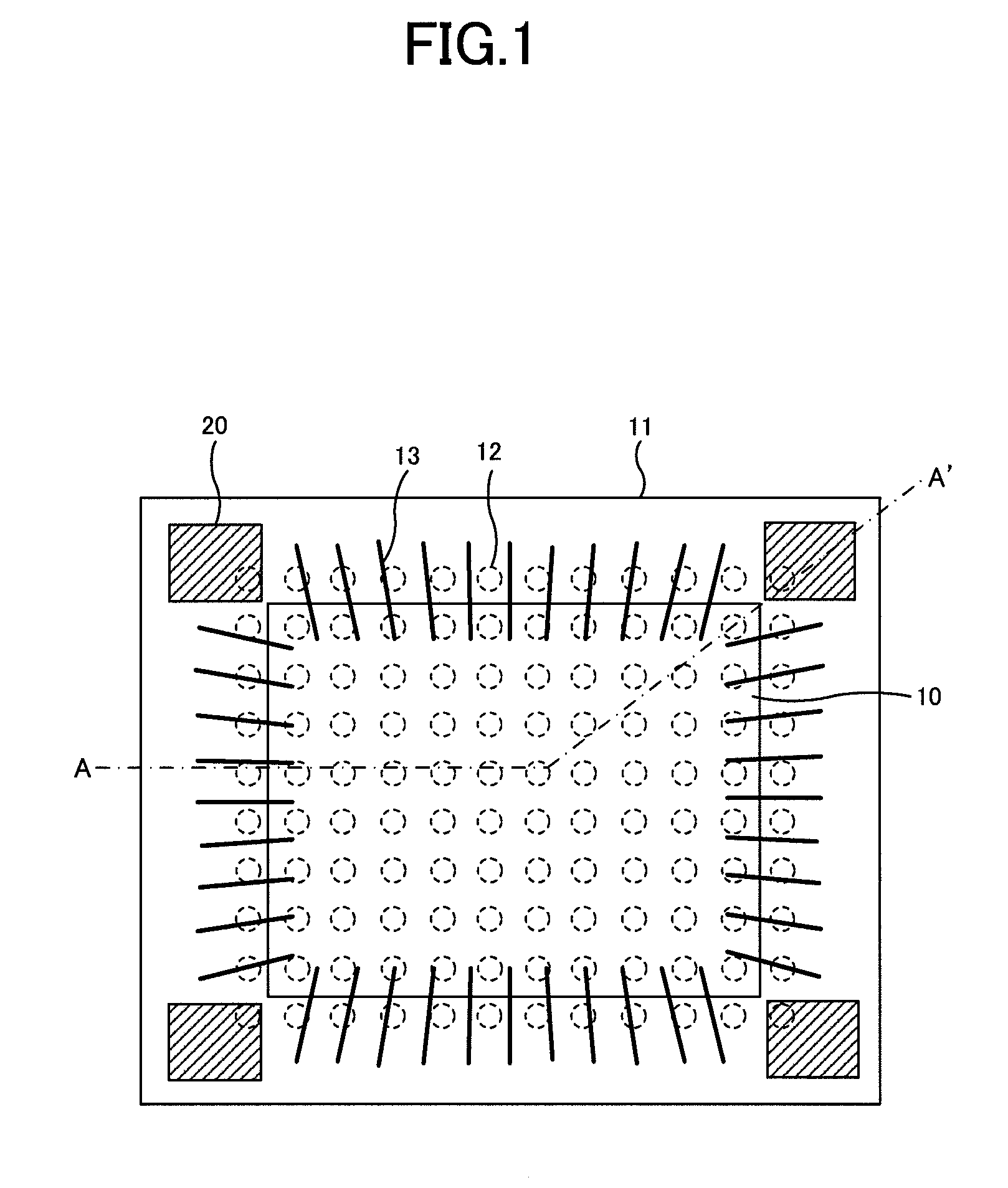
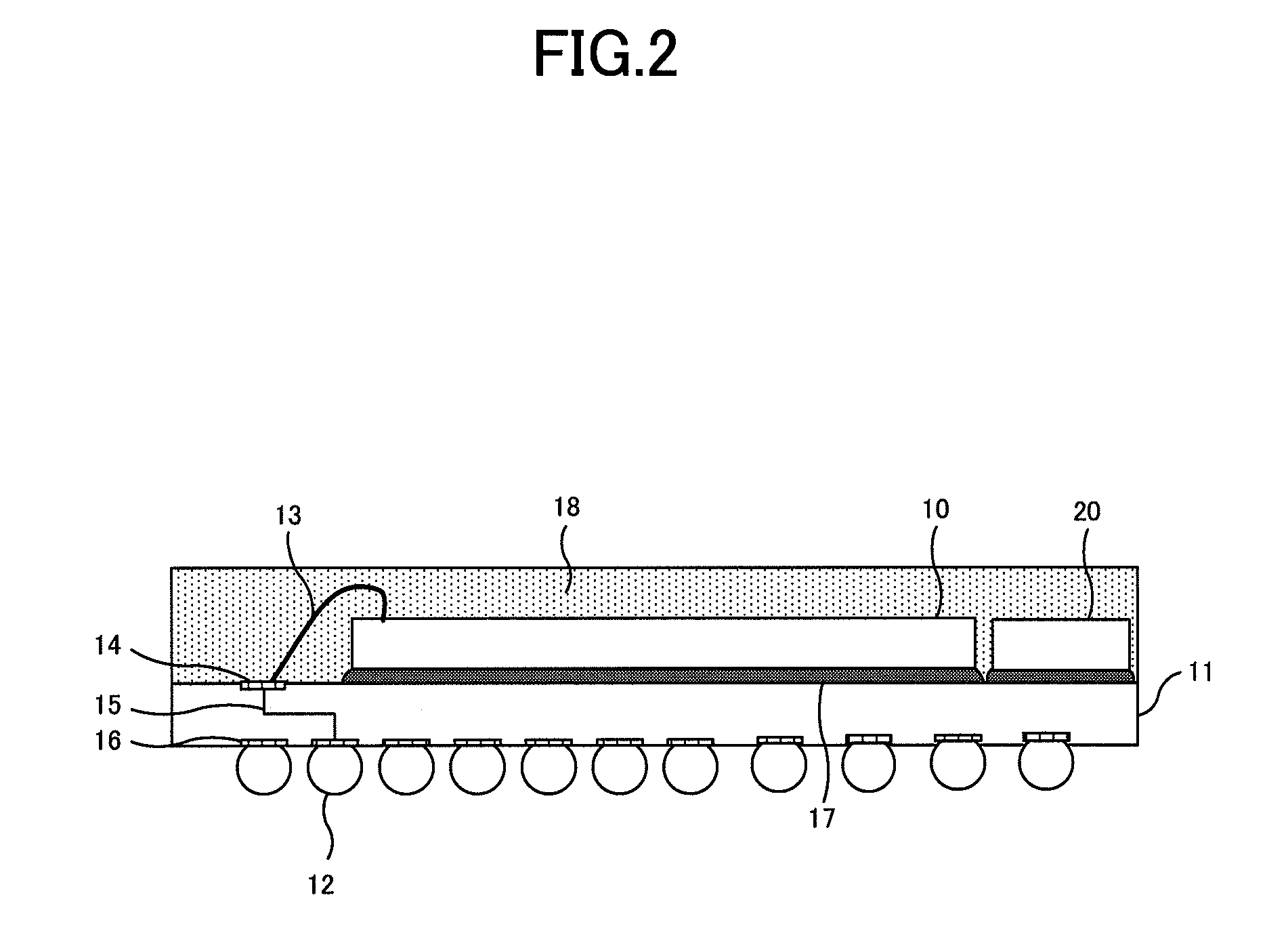
[0031]A semiconductor device of a first embodiment will be described with reference to FIGS. 1 to 4. Regarding a structure of the semiconductor device of the first embodiment, FIG. 1 shows a plan view and FIG. 2 shows a cross-sectional view along a line A-A′ in FIG. 1. The semiconductor device of the first embodiment has a structure in which a semiconductor chip 10 with a predetermined electronic circuit is mounted on a central region of a top surface of a package substrate 11. The package substrate 11 is formed in a rectangle larger than the size of the semiconductor chip 10, and four dummy chips 20 whose size is smaller than the semiconductor chip 10 are mounted at positions close to four corner portions around the semiconductor chip 10 in a peripheral region of the top surface of the package substrate 11. The function of these dummy chips 20 will be described later. A plurality of bump electrodes 12 for connection with an external circuit board are formed in a matrix arrangement ...

second embodiment

[0042]Next, a semiconductor device of a second embodiment will be described with reference to FIGS. 5 and 6. Regarding a structure of the semiconductor device of the second embodiment, FIG. 5 shows a plan view and FIG. 6 shows a cross-sectional view along a line A-A′ in FIG. 5. In the semiconductor device of the second embodiment, the basic structure including the semiconductor chip 10 and the package substrate 11 is the same as that in the first embodiment. Meanwhile, in the second embodiment, four dummy chips 21 each having a shape different from that of the dummy chip 20 of the first embodiment are arranged in regions close to the four corner portions around the semiconductor chip 10.

[0043]Each dummy chip 21 of the second embodiment is formed in a rectangle larger than the size of the dummy chip 20 in FIG. 1. That is, two sides of the dummy chip 21 are located to overlap the two sides of the package substrate 11 as shown in FIG. 5. Further, each dummy chip 21 is mounted so that i...

third embodiment

[0045]Next, a semiconductor device of a third embodiment will be described with reference to FIG. 7. FIG. 7 shows a plan view of the semiconductor device of the third embodiment. In the semiconductor device of the third embodiment, the basic structure including the semiconductor chip 10 and the package substrate 11 is the same as that in the first embodiment. Meanwhile, in the third embodiment, two dummy chips 22 are arranged in two regions close to both two adjacent corner portions of the four corner portions around the semiconductor chip 10. In addition, a cross sectional structure of the semiconductor device of the third embodiment can be similarly shown as in FIG. 2.

[0046]The dummy chips 22 of the third embodiment are located along opposite two sides of the rectangular package substrate 11. Thus, each dummy chip 22 is formed in a rectangle having two short sides of the same length as that in FIG. 1 and two long sides of a length close to the length of the package substrate 11. T...


PUM


Abstract

A semiconductor device comprises a package substrate, a semiconductor chip, a plurality of bump electrodes and one or more dummy chips. The semiconductor chip is mounted on one surface of the package substrate. The bump electrodes are the other surface of the package substrate and electrically connected to the semiconductor chip through a wiring structure. Each of the dummy chips is mounted on a predetermined region close to a corner portion of the semiconductor chip on the one surface of the package substrate.In the semiconductor chip, the dummy chips are formed of material having the same or similar coefficient of thermal expansion as that of the semiconductor chip. Therefore the stress caused by a difference between coefficients of thermal expansion is suppressed so as to improve connection reliability.

Description

BACKGROUND OF THE INVENTION[0001]1. Field of the Invention[0002]The present invention relates to a semiconductor device having a semiconductor chip mounted on a package substrate, and particularly relates to a semiconductor device having a structure for improving connection reliability of bump electrodes formed on a back surface of the package substrate, and manufacturing method thereof.[0003]2. Description of Related Art[0004]Semiconductor devices have been conventionally used in which a large number of bump electrodes are formed on a back surface of a package substrate and a semiconductor chip is mounted on the package substrate. Such semiconductor devices particularly have a problem of fracture of bump electrodes located in the vicinity of an outer portion of the semiconductor chip among the bump electrodes on the package substrate. Generally, in the semiconductor chip, a difference between coefficients of thermal expansion is larger than that of the package substrate or resin, a...

Claims


Application Information

Patent Timeline
Patent Type & Authority Patents(United States)
IPC IPC(8): H01L23/48H01L29/40
CPCH01L23/16H01L23/49833H01L23/562H01L24/97H01L23/3128H01L2924/10253H01L24/28H01L24/45H01L24/48H01L24/49H01L24/85H01L2224/45144H01L2224/48091H01L2224/48227H01L2224/48463H01L2224/49171H01L2224/73265H01L2224/85201H01L2224/85205H01L2224/92H01L2224/97H01L2924/01004H01L2924/01014H01L2924/01027H01L2924/01079H01L2924/078H01L2924/07802H01L2924/15184H01L2924/15311H01L2924/3511H01L2924/01033H01L2924/01006H01L2924/01005H01L2224/32225H01L2924/00014H01L2224/85H01L2224/83H01L2224/92247H01L2924/00H01L2924/3512H01L2924/00012H01L24/73H01L2924/181
Inventor FUJII, SEIYA
Owner MICRON TECH INC
Why Eureka
Try Eureka