Manufacturing method for a semiconductor device, semiconductor device, circuit substrate and electronic device

a manufacturing method and semiconductor technology, applied in the direction of semiconductor/solid-state device details, digital storage, instruments, etc., can solve the problems of excessive stress on the portions, damage to cracks formed by minute fissures on the rear surface of the semiconductor wafer, so as to improve the strength and thinning effect and improve reliability

Active Publication Date: 2006-12-21
SAMSUNG ELECTRONICS CO LTD
View PDF12 Cites 32 Cited by
  • Summary
  • Abstract
  • Description
  • Claims
  • Application Information

AI Technical Summary

Benefits of technology

[0024] An advantage of some aspects of the invention is to provide a manufacturing method for a semiconductor device, a semiconductor device, a circuit substrate and electronic device, which can efficiently remove a chipped or damaged layer in the manufacturing process for a semiconductor device, and which can suppress damage caused by the stress concentration at the time of thinning the semiconductor wafer.

Problems solved by technology

However, in the above described manufacturing method, damaged layers having minute fissures (cracks) are formed on the rear surface of the semiconductor wafer, caused by back grind processing.
Furthermore, there has been the problem in that, if the semiconductor rear surface damaged layer is left in its existent state, and if the manufacturing of the semiconductor device is continued, beginning with cracking of the damaged layer, the semiconductor element becomes completely broken.
Furthermore, there has been the problem in that, during dicing processing, in order to mechanically remove the semiconductor wafer by bevel cutting and the similar, minute cracking and chipping and the similar has been generated in the area of the cut surface of the semiconductor wafer.
In addition, since the semiconductor wafer is thin, there has been the problem of excessive stress on the portions in which cracking, chipping and the similar are generated.
However, in the above disclosed method, there are the following problems.
(1) In the method disclosed in Unexamined Japanese Unexamined Patent Application First Publication No. 2000-228389, there has been the problem in that, order to remove the damaged layer formed on the semiconductor wafer rear surface by grinding and polishing through plasma etching, a longer time is required than with other etching methods.
(2) In the method disclosed in Japanese Unexamined Patent Application First Publication No. 2002-93752, there has been difficulty in handling the wafer to accomplish semi (full) dicing after thin processing the semiconductor wafer.
(3) Furthermore, in the above described method, when thinning the semiconductor device, stress easily concentrates in end portions of the semiconductor device, and the semiconductor device is damaged and broken.
Generally, after thinning a semiconductor wafer by means of back grinding, if a second groove is formed by dicing the rear surface of the semiconductor wafer, then cracks (a damaged layer) are formed on the rear surface of the semiconductor wafer and the inner wall surface of the second groove.
Furthermore, even if the center of the second groove is slightly sifted from the center of the first groove, the formation region of the second groove will be within the formation region of the first groove, and highly precise position determination accuracy is unnecessary to make the easily formed second groove.

Method used


Image

  • Manufacturing method for a semiconductor device, semiconductor device, circuit substrate and electronic device
  • Manufacturing method for a semiconductor device, semiconductor device, circuit substrate and electronic device
  • Manufacturing method for a semiconductor device, semiconductor device, circuit substrate and electronic device

Examples


first embodiment

[0107] Semiconductor Wafer

[0108] First of all, an explanation is provided concerning the semiconductor wafer before the individualizing of the semiconductor devices.

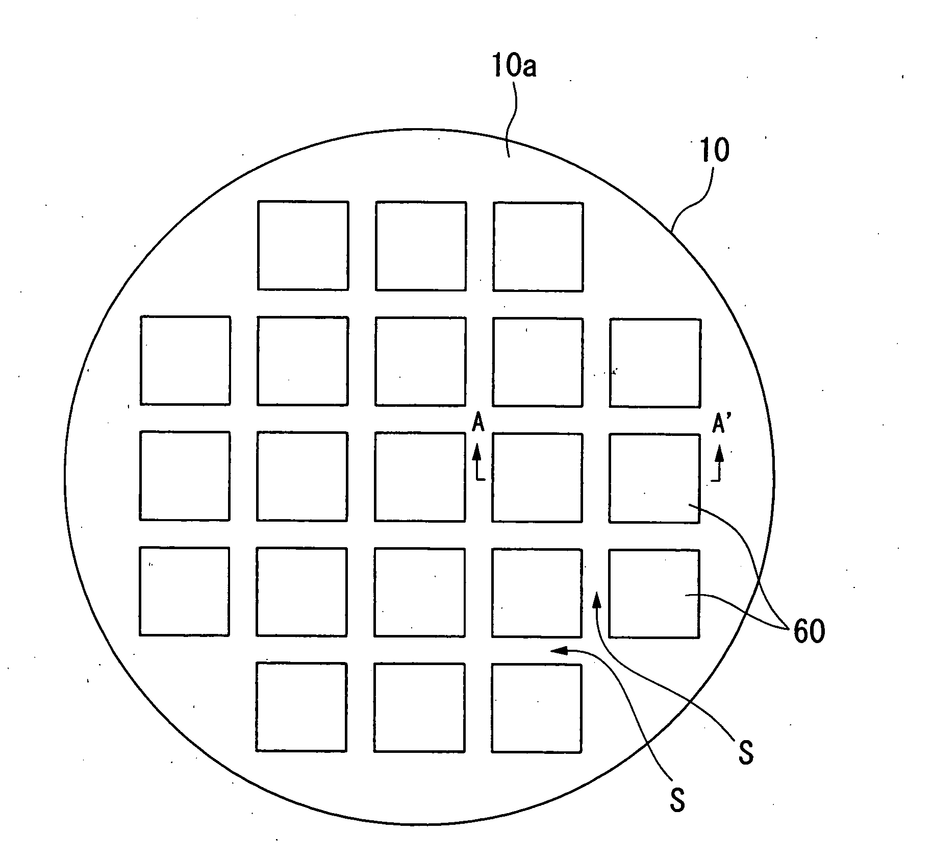
[0109]FIG. 1 is a plan view that schematically shows the semiconductor wafer 10 on which a plurality of semiconductor regions 60 is formed.

[0110] Semiconductor wafer 10 is formed from silicon material on which is formed semiconductor regions 60.

[0111] On the active surface 110a of the semiconductor wafer 1 is formed an accumulation circuit (integrated circuit) including a transistor, memory element and other semiconductor elements for each of the semiconductor regions 60.

[0112] In the first embodiment, the semiconductor region 60 is a region which becomes a semiconductor device by below described manufacturing method, and means a region formed on a semiconductor wafer before the individualizing of the semiconductor devices.

[0113] The semiconductor element is not formed on the rear surface 10b of the opposite side o...

second embodiment

[0225] An explanation of the second embodiment is provided hereafter, with reference to the drawings.

[0226] In the second embodiment, the first groove 20 is filled with resin, and a resin layer is formed into the first groove 20.

[0227] Therefore, the manufacturing process of the semiconductor device 61 of the second embodiment differs from the manufacturing process of the semiconductor device 61 of the first embodiment.

[0228] In the second embodiment, a detailed explanation is provided concerning the forming process of a resin layer into the first groove 20, and a process after the forming process of a resin layer within the first groove 20.

[0229] The same reference numerals are applied to construction components which are common to those of the semiconductor device 61 of the first embodiment, simplifying the explanation of other processes.

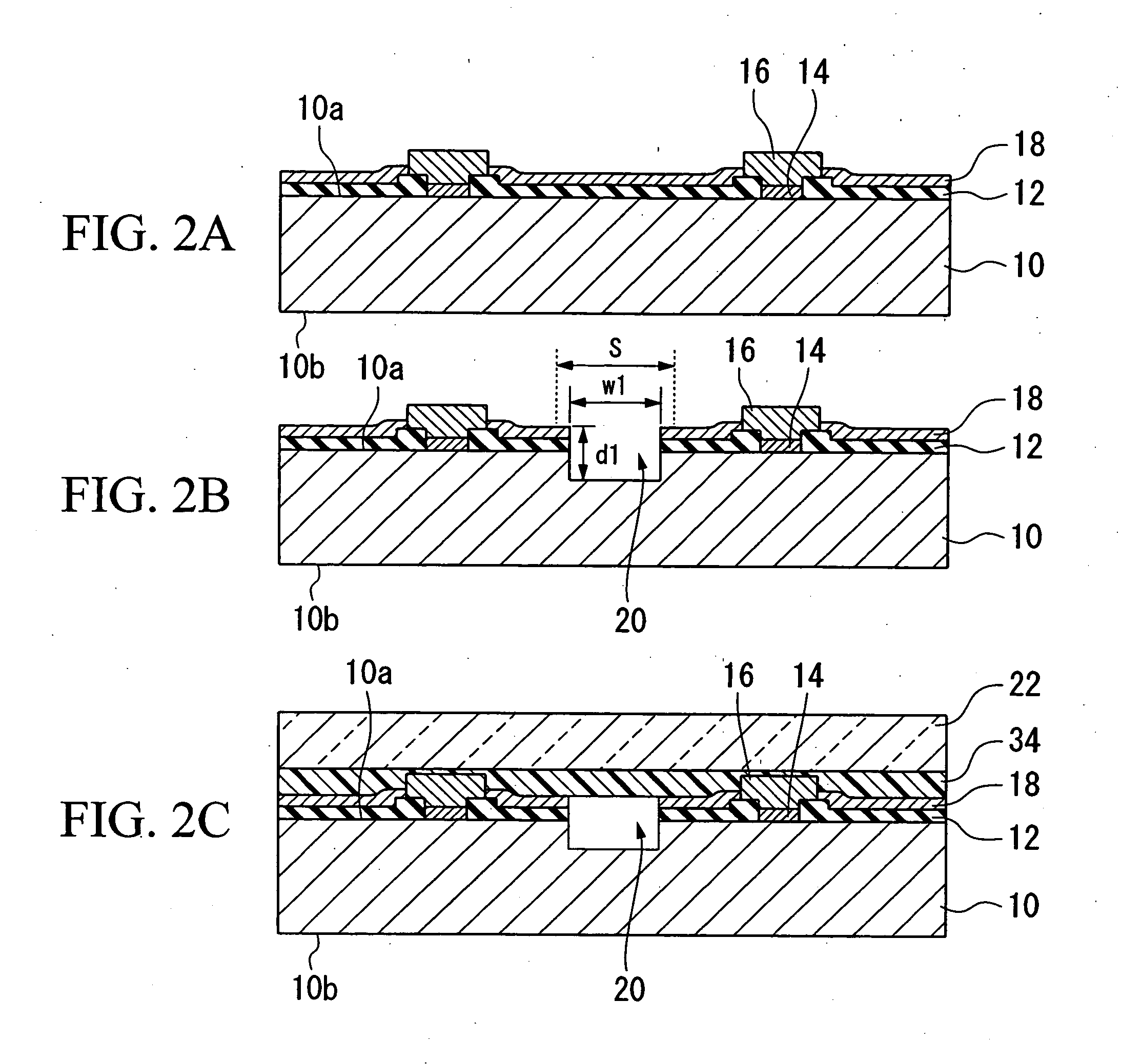
[0230] Electrode and First Groove Forming Processes

[0231] First of all, as shown in FIG. 5A, electrode pad 14 is formed on the semiconducto...

third embodiment

[0278] An explanation of this embodiment is provided next, with reference to the drawings.

[0279] In the manufacturing method for the semiconductor device 61 of the third embodiment, there is a difference in comparison with the manufacturing method for the semiconductor device 61 of the first embodiment, in the point that TEG is not formed in the respective cutting regions S of semiconductor regions 60 in the semiconductor wafer.

[0280] In the third embodiment, the same reference numerals are applied to and explanations omitted from processes and compositions which are the same as those of the first embodiment, and explanations are only provided for parts which differ from those of the first embodiment.

[0281]FIGS. 8A to 9C are cross-sectional views that show the forming of semiconductor devices 61 in which the semiconductor wafer 10 has been individualized for each semiconductor region 60.

[0282] Semiconductor Wafer

[0283] First of all, an explanation is provided concerning semicon...


PUM


Abstract

A manufacturing method for a semiconductor device, includes: preparing a semiconductor wafer having an active surface and a rear surface; forming a plurality of semiconductor regions, each of which having semiconductor elements formed on the active surface of the semiconductor wafer; forming cutting regions on the outer periphery of the semiconductor regions on the active surface of the semiconductor wafer; forming, on the cutting region, a first groove which does not penetrate the semiconductor wafer; forming, on the rear surface of the semiconductor wafer, a second groove which does not penetrate to the first groove in the position corresponding to the cutting region; decreasing a thickness of the semiconductor wafer, connecting the first groove and the second groove, and dividing each of the semiconductor regions from the semiconductor wafer by executing isotropic etching to the rear surface of the semiconductor wafer; and obtaining a plurality of individual semiconductor devices.

Description

CROSS-REFERENCE TO RELATED APPLICATION [0001] This application claims priority to Japanese Patent application No. 2005-177495, filed Jun. 17, 2005, and Japanese Patent application No. 2005-335459, filed Nov. 21, 2005, the contents of which are incorporated herein by reference. BACKGROUND [0002] 1. Technical Field [0003] The present invention relates to the manufacturing method for a semiconductor device, a semiconductor device, a circuit substrate and an electronic device. [0004] 2. Related Art [0005] In recent years, there has been a demand to miniaturize and reduce the weight of portable telephone devices, notebook portable computers and portable electronic devices such as a PDA (personal digital assistant) and the similar. [0006] Accompanying the demand for miniaturization and weight reduction, there has also been demand to limit the packaging space for each type of electronic product, such as semiconductor devices and the similar, provided within the electronic devices, as well ...

Claims


Application Information

Patent Timeline
Patent Type & Authority Applications(United States)
IPC IPC(8): G11C29/00H01L29/06H01L23/02G11C7/00
CPCH01L24/90H01L25/0657H01L2224/83192H01L2224/81191H01L2224/2919H01L2224/32225H01L2224/26145H01L2924/01033H01L2924/01023H01L2924/01006H01L24/83H01L24/81H01L24/32H01L23/3178H01L21/78H01L21/6835H01L2924/14H01L2924/10158H01L2924/10157H01L2924/01078H01L2221/68318H01L2221/6834H01L2224/16225H01L2224/27013H01L2224/73204H01L2224/8121H01L2224/81815H01L2224/83051H01L2224/83851H01L2224/90H01L2225/06513H01L2924/01005H01L2924/01013H01L2924/01029H01L2924/10155H01L2924/00H01L2924/3512H01L2924/0665H01L2924/00014H01L2224/0554H01L2224/05568H01L2224/05573H01L2224/05599H01L2224/0555H01L2224/0556H01L21/302H01L21/304
Inventor FUKAZAWA, MOTOHIKO
Owner SAMSUNG ELECTRONICS CO LTD
Why Eureka
Try Eureka