Circuit device and manufacturing method thereof

Inactive Publication Date: 2005-09-29
SANYO ELECTRIC CO LTD
View PDF3 Cites 12 Cited by
  • Summary
  • Abstract
  • Description
  • Claims
  • Application Information

AI Technical Summary

Benefits of technology

[0031] Furthermore, compared to the case of mounting on a ceramic substrate, a step of forming a through-hole, a step of printing a conductor and the like can be omitted. There is an advantage

Problems solved by technology

Specifically, there are problems that, for the connection of the passive element, the multi-layered structure has to be formed by increasing costs and the number of production process, or the mounting area has to be further increased.
Furthermore, in the case of fixing by use of the solder material, a device having a structure subjected to plastic molding, has the following problems.
This is because, if the reflow temperature reaches the melting point of solder or more, solder is remelted to cause short circuit or package destruction.
Moreover, if the package is distorted by heat generated after plastic m

Method used


Image

  • Circuit device and manufacturing method thereof
  • Circuit device and manufacturing method thereof
  • Circuit device and manufacturing method thereof

Examples


Example

[0041] With reference to FIGS. 1 to 8, an embodiment of a circuit device of the present invention will be described.

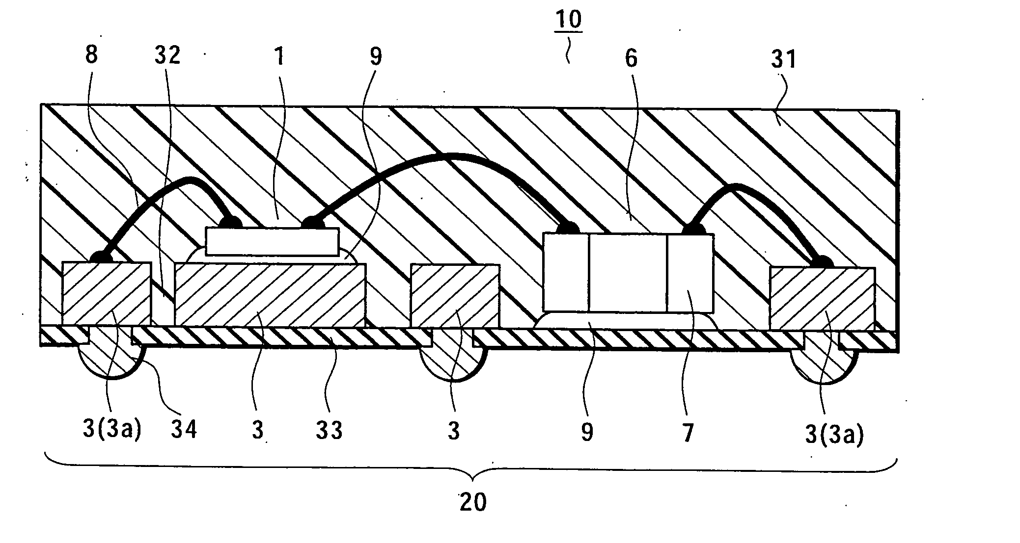
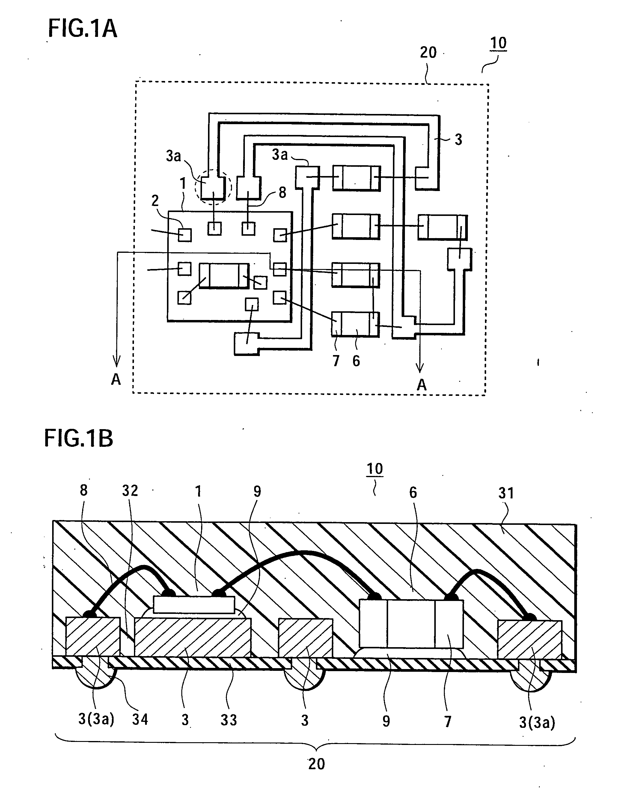
[0042]FIGS. 1A and 1B show the circuit device of this embodiment. FIG. 1A is a plan view, and FIG. 1B is a cross-sectional view along the line A-A in FIG. 1A.

[0043] The circuit device 10 of this embodiment includes a semiconductor element 1, conductive patterns 3, passive elements 6, and bonding wires 8.

[0044] As shown in FIG. 1A, in the circuit device 10 of this embodiment, at least the semiconductor element 1 such as an IC, the conductive patterns 3, and the passive elements 6 are embedded and supported by use of an insulating resin in a package region 20 indicated by the broken line. Thus, a predetermined circuit is formed. The conductive pattern 3 has a pad part 3a on its end, to which the bonding wire 8 is fixed.

[0045] In this embodiment, the passive element 6 is a chip element having electrode parts 7 on its both ends, such as a chip resistor, a chip condense...


PUM


Abstract

In the case of mounting a passive element in a circuit device, since an electrode part is tin-plated, the passive element is fixed to a mounting land part by use of a solder material, and wires cannot intersect with each other in a single layer. Accordingly, there are problems such as an increase in a mounting area, a restriction to a reflow temperature in mounting on a printed board, and deterioration of reliability due to solder crack after packaging. The electrode part of the passive element is gold-plated, and a bonding wire is directly fixed to the electrode part. Thus, a packaging density can be improved. Moreover, a package structure using no supporting substrate is adopted, and the passive element is bonded to an isolation trench. Thus, even in a structure having the bonding wire fixed therein, an increase in a package thickness is suppressed.

Description

BACKGROUND OF THE INVENTION [0001] 1. Field of the Invention [0002] The present invention relates to a circuit device including a passive element and a manufacturing method thereof, and more particularly relates to a circuit device having an improved wiring density and a manufacturing method thereof. [0003] 2. Description of the Related Art [0004] With reference to FIGS. 9A and 9B, a conventional circuit device will be described. FIG. 9A is a plan view of the circuit device, and FIG. 9B is a cross-sectional view along the line B-B in FIG. 9A. [0005] As shown in FIG. 9A, a semiconductor element 101 such as an IC, for example, and a plurality of conductive patterns 103 are arranged in a predetermined package region 120 on a supporting substrate 110, for example. The conductive patterns 103 include a pad part 103a to which a bonding wire 108 or the like is fixed, and / or mounting land parts 103b to which both electrode parts 107 of a passive element 106 are fixed. The passive element 10...

Claims


Application Information

Patent Timeline
IPC IPC(8): H01C1/14H01L25/00H01L21/48H01L21/52H01L23/02H01L23/12H01L23/31H01L23/48H01L23/488H01L23/538H01L25/16H05K1/02H05K1/18H05K3/06H05K3/28H05K3/32
CPCH01L21/4832H01L23/3107H01L2924/07802H01L2224/45144H01L2224/92247H01L23/3128H01L23/5387H01L25/16H01L25/165H01L2224/48195H01L2924/01046H01L2924/01078H01L2924/01079H01L2924/15311H01L2924/19041H01L2924/19105H01L2924/30107H05K1/0231H05K1/185H05K3/06H05K3/284H05K3/328H05K2201/10636H05K2203/0369H05K2203/049H05K2203/1476H01L24/48H01L2224/73265H01L2924/00H01L2224/45124H01L2924/00014H01L24/45H01L2924/181H01L2224/05554H01L2924/19104H01L2224/48247H01L2224/97H01L2224/32245H01L2224/48265H01L24/49H01L2224/49171Y02P70/50H01L2224/05599H01L2924/00012B26F3/04B26D1/0006B26D2001/0066
Inventor KATO, ATSUSHI
Owner SANYO ELECTRIC CO LTD
Why Eureka
Try Eureka