Method of manufacturing a super-junciton semiconductor device

Active Publication Date: 2014-08-28
FUJI ELECTRIC CO LTD
View PDF2 Cites 24 Cited by
  • Summary
  • Abstract
  • Description
  • Claims
  • Application Information

AI Technical Summary

Benefits of technology

The present invention provides a method of manufacturing a super-junction semiconductor device using a technique of embedding in trenches to form high concentration layer with high accuracy. This method eliminates repeated redundant steps, resulting in low manufacturing costs. In addition, enhanced impurity concentration in the surface side of the super-junction parts makes dV / dt smaller and improves the trade-off relationship between the dV / dt and the Eoff, at low manufacturing costs. Using a heavy particle irradiation technique for forming a high concentration region forms the impurity concentration and thickness in the high concentration region with high accuracy, improving the rate of non-defective products, reducing manufacturing costs.

Problems solved by technology

Consequently, a shortened current path of the n− drift layer lowers a drift resistance and thus reduces actual ON resistance of a MOSFET.
On the contrary, a semiconductor device exhibiting a high withstand voltage has a thick n− drift layer and a high ON resistance, resulting in large conduction loss.
This construction makes the extension of depletion layer in the turning OFF process difficult without changing an external gate resistance connected to the gate terminal of the super-junction semiconductor device.
An enlarged gate resistance, however, elongates the time for drawing out the charges from a gate capacitance including a mirror capacitance of the super-junction semiconductor device in a turning OFF process, resulting in increased turning OFF loss, i.e., Eoff.
This procedure takes a long time and raises manufacturing costs.
The trench embedding method is also costly when the high concentration layer with a homogeneous impurity concentration is formed by epitaxial growth process.
The epitaxial growth process is difficult to control an impurity concentration and thickness of the high concentration layer with high accuracy.

Method used


Image

  • Method of manufacturing a super-junciton semiconductor device
  • Method of manufacturing a super-junciton semiconductor device
  • Method of manufacturing a super-junciton semiconductor device

Examples


embodiment example 1

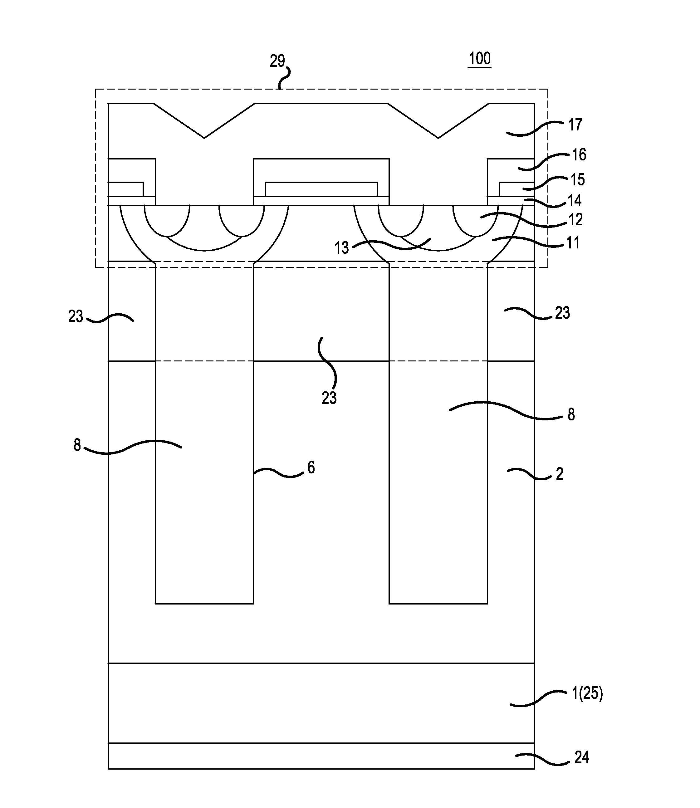
[0066]FIGS. 1 through 9 show a method of Embodiment Example 1 of the present invention for manufacturing super-junction semiconductor device 100 and are sectional views of essential parts presented in the sequence of manufacturing steps. Although the following description of Embodiment Example 1 is made basically about a super-junction MOSFET with a withstand voltage of 600 V class, the present invention can be applied to any devices with other withstand voltage classes by appropriately adjusting film thicknesses, dimensions, and other parameters.

[0067]In the following description, a first conductivity type is an n type and a second conductivity type is a p type. However, the conductivity type can be reversed.

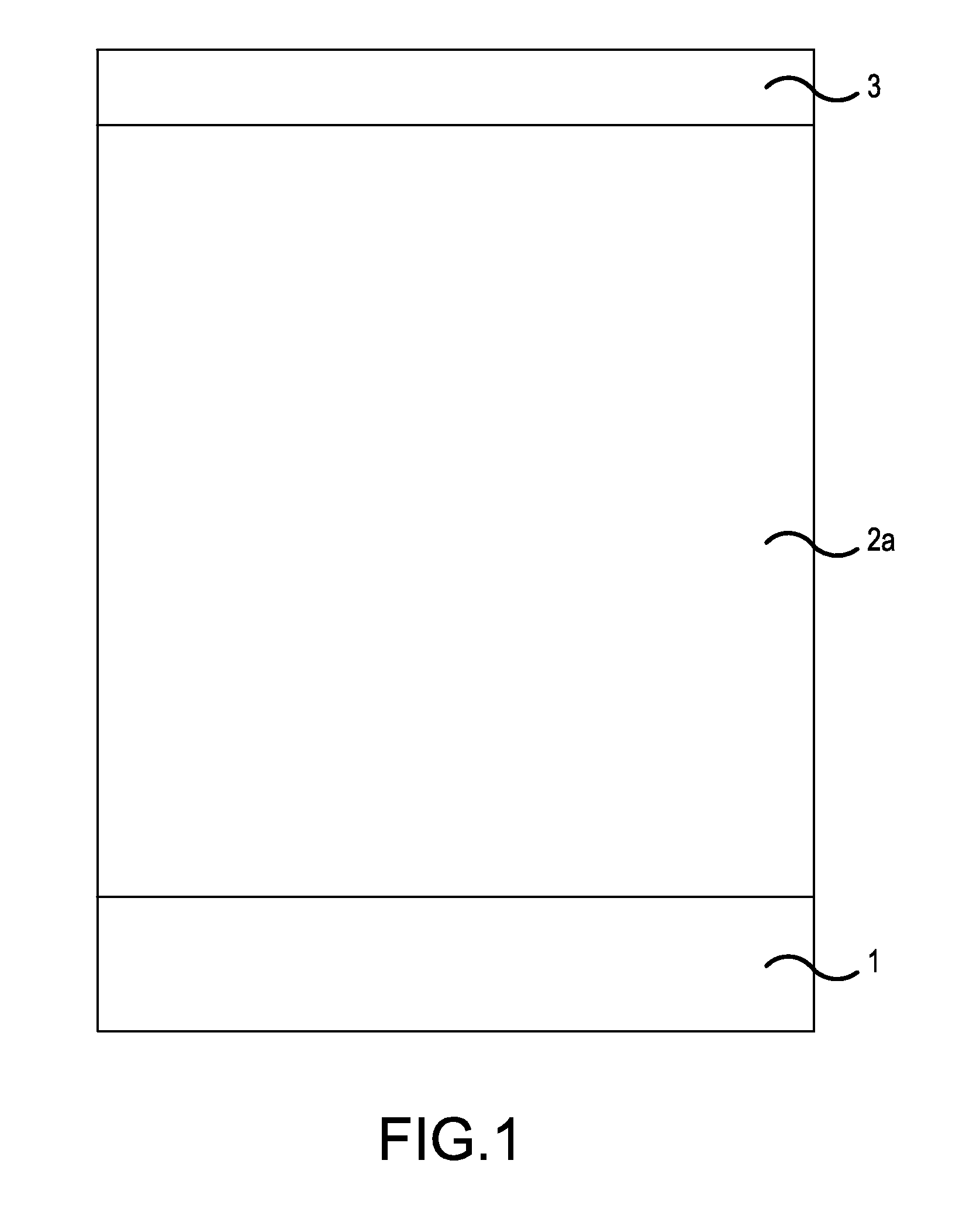
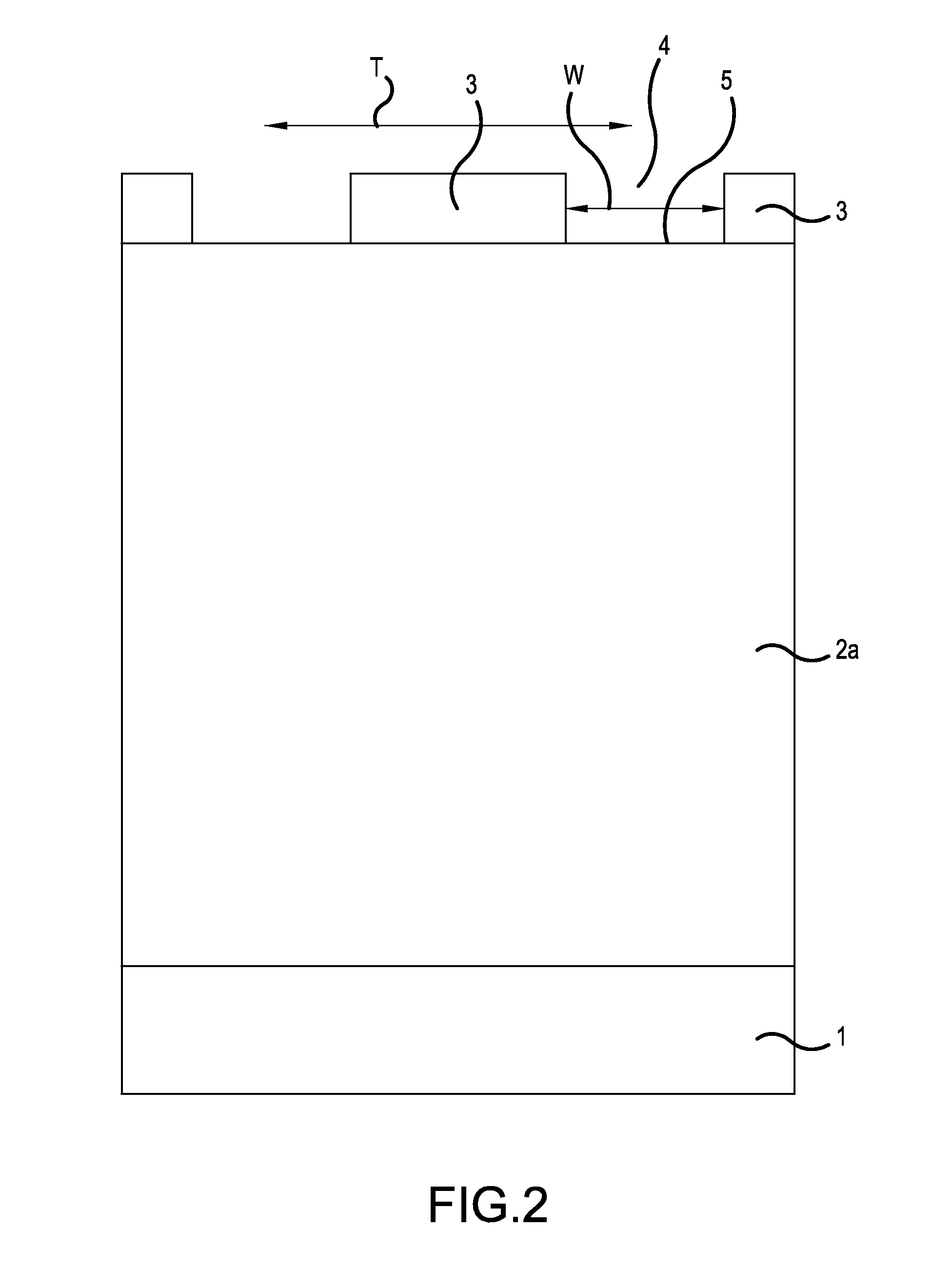
[0068](1) First, as shown in FIG. 1, on n type semiconductor substrate 1 of silicon with a thickness of several hundred microns, n type semiconductor layer 2a with a thickness of about 45 μm is formed by epitaxial growth, and on n type semiconductor layer 2a, oxide film 3 of Si...

embodiment example 2

[0090]FIG. 12 is a sectional view showing an essential part of a super-junction semiconductor device 200 in a step of manufacturing the device 200 according to a second embodiment of the invention. This drawing corresponds to FIG. 7 in Embodiment Example 1. This Embodiment Example 2 differs from Embodiment Example 1 in that Embodiment Example 2 uses irradiation particles of helium ions 27, i.e., 3He++ and 4He++ in place of protons 18. In the case of helium ions 27, a temperature necessary for donorization is about 500° C. and higher than in the case of protons 18. Consequently, damage to a an electrode is a concern. In order to cope with this problem, the particle irradiation and subsequent heat treatment are favorably carried out before forming the drain electrode and the source electrode.

[0091]The helium ion irradiation has similar effects as the proton irradiation. FIG. 12 indicates helium ion irradiation 26 and helium ion irradiation layer 28.

embodiment example 3

[0092]FIG. 16 and FIG. 17 illustrate a method of manufacturing a super-junction semiconductor device 300 according to the third embodiment of the present invention, in which FIG. 16 is a sectional view of an essential part of the device in a manufacturing step corresponding to FIG. 7 in Embodiment Example 1 and FIG. 17 is a plan view of a shielding mask used in the step of forming the structure of FIG. 16.

[0093]N type semiconductor layer 2 is subjected to proton irradiation, but p type semiconductor layer 8 is prevented from irradiation using shielding mask 41 made of aluminum. The shielding mask is not limited to aluminum but chromium, gold, or other materials that can shield the irradiating ions can be used.

[0094]Because p type semiconductor layer 8 is not irradiated by protons, the p type impurity concentration does not decrease, which improves charge balance as compared with the case of Embodiment Example 1. Thus, a necessary withstand voltage is readily secured and the n type i...


PUM


Abstract

A method of manufacturing a super-junction semiconductor device is disclosed that allows forming a high concentration layer with high precision and improves the trade-off relationship between the Eoff and the dV / dt using a trench embedding method. The method comprises a step of forming a parallel pn layer using a trench embedding method and a step of forming a proton irradiated layer in the upper region of the pn layer. Then, heat treatment is conducted on the proton irradiated layer for transforming the protons into donors to form a high concentration n type semiconductor layer. Forming the high concentration n type semiconductor layer by means of proton irradiation allows forming a high concentration n type semiconductor layer with an impurity concentration and thickness with high precision as compared with forming the layer by means of an epitaxial growth process.

Description

[0001]This application is based on, and claims priority to, Japanese Patent Application No. 2013-034487, filed on Feb. 25, 2013, contents of which are incorporated herein by reference.BACKGROUND OF THE INVENTION[0002]A. Field of the Invention[0003]The present invention relates to a method of manufacturing a power semiconductor device such as a MOSFET, and in particular, to a method of manufacturing a super-junction semiconductor device having a super-junction structure (also called a parallel pn column structure), a drift layer which is constructed with n type columns and p type columns extending in a direction perpendicular to a principal surface of a semiconductor substrate and arranged alternately in the direction parallel to the principal surface.[0004]B. Description of the Related Art[0005]The following patent documents will be discussed herein:Patent Document 1—Japanese Unexamined Patent Appn. Pub. No. 2001-119022Patent Document 2—U.S. Pat. No. 5,216,275Patent Document 3—Inter...

Claims


Application Information

Patent Timeline
IPC IPC(8): H01L29/66H01L21/265
CPCH01L29/66477H01L21/265H01L21/263H01L21/324H01L29/66712H01L29/7802H01L29/7813H01L29/0634H01L29/0878H01L29/1095
Inventor YAMADA, MICHIYAFUJIHARA, TATSUHIKO
Owner FUJI ELECTRIC CO LTD
Why Eureka
Try Eureka