
Semiconductor device and method of manufacturing the same

Inactive Publication Date: 2002-09-19
RENESAS ELECTRONICS CORP
View PDF0 Cites 15 Cited by
  • Summary
  • Abstract
  • Description
  • Claims
  • Application Information

AI Technical Summary

Benefits of technology

[0177] According to the first aspect of the present invention, since at least one of the first to the third control electrodes internally includes an impurity layer of the second conductivity type having a concentration distribution in the direction of depth, it is possible to change the impurity concentrations of the control electrodes independently of each other among the first to the third types of transistors which have different characteristics from each other (e.g., having different required specifications from each other), and hence, it is possible to change the effective thicknesses of the gate oxide films, so that threshold values are set. Further, since it is possible to change the effective thicknesses of the gate oxide films by changing the impurity concentrations of the control electrodes, it is not necessary to form the gate oxide films of the transistors which have different breakdown voltages from each other to have different thicknesses from each other.
[0206] Accordingly, an object of the present invention is to provide for a semiconductor device in which there is no trade-off relationship between a threshold value and a diffusion layer leak and it is not necessary to form gate oxide films at more than one steps, and to provide for a method of manufacturing such a semiconductor device.

Problems solved by technology

That is, when ions are to be implanted into the semiconductor substrate, in particular, when implantation at a high dose is to be executed, this causes crystal deterioration of the semiconductor substrate.

Method used


Image

  • Semiconductor device and method of manufacturing the same
  • Semiconductor device and method of manufacturing the same
  • Semiconductor device and method of manufacturing the same

Examples


Embodiment Construction

[0255] In general, a gate electrode forming a MOS transistor is doped with an N-type impurity or a P-type impurity. This aims at reducing the resistance of a gate by means of doping with the impurity. Further, whether to use an N-type impurity or a P-type impurity depends on the type of a well layer. That is, when a P-type gate electrode is selected for an N-type well or an N-type gate electrode is selected for a P-type well, it is possible to suppress a threshold value.

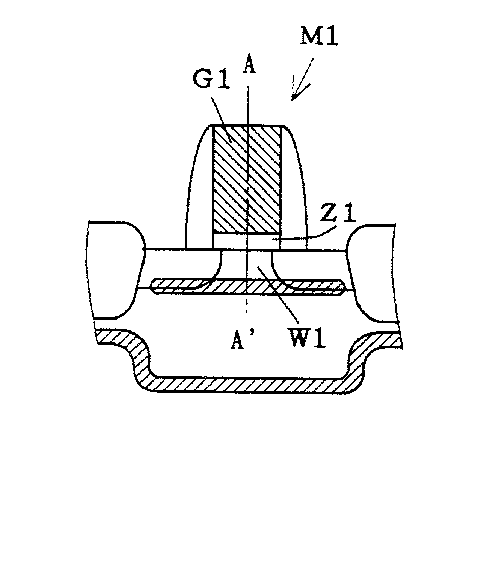
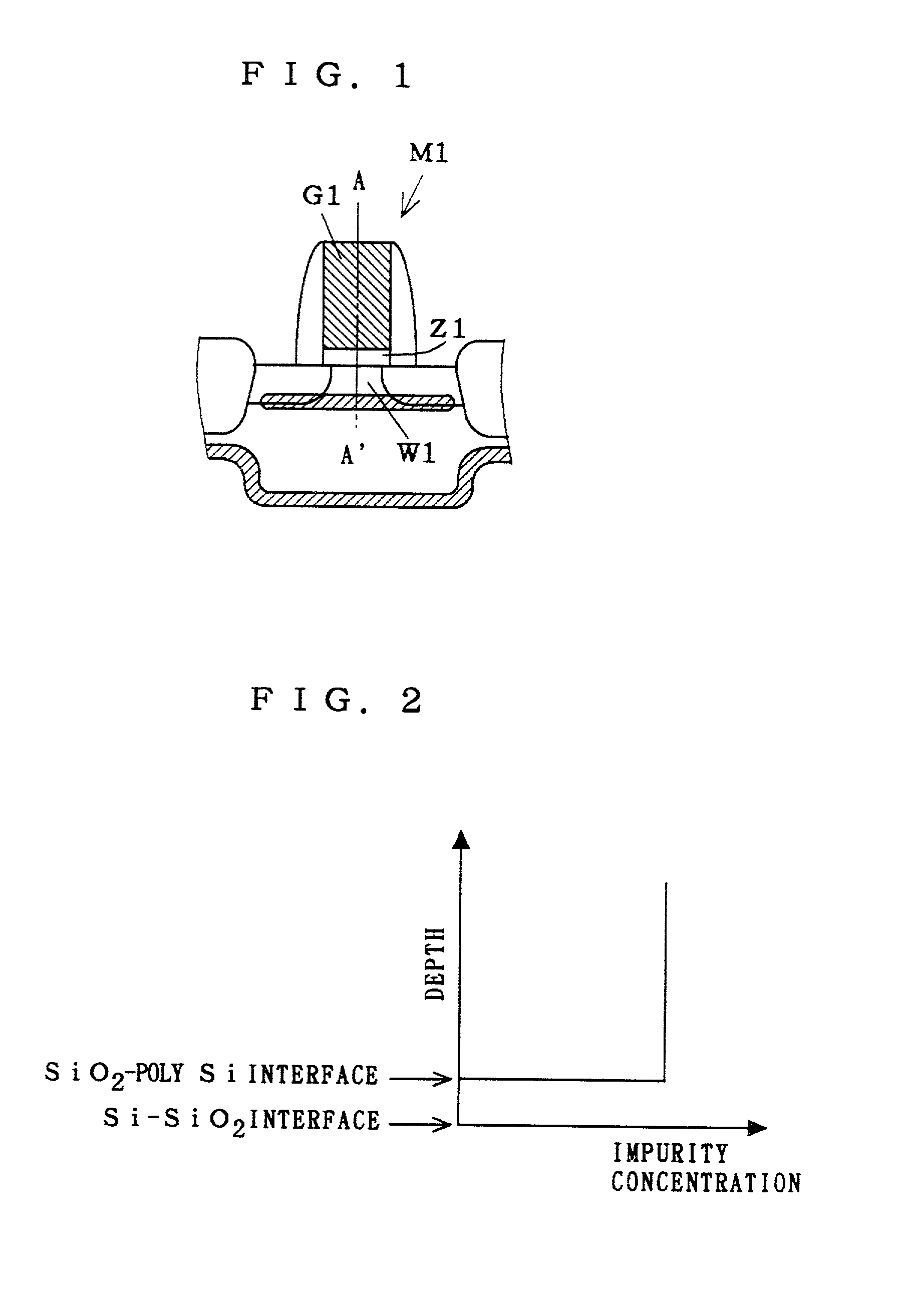
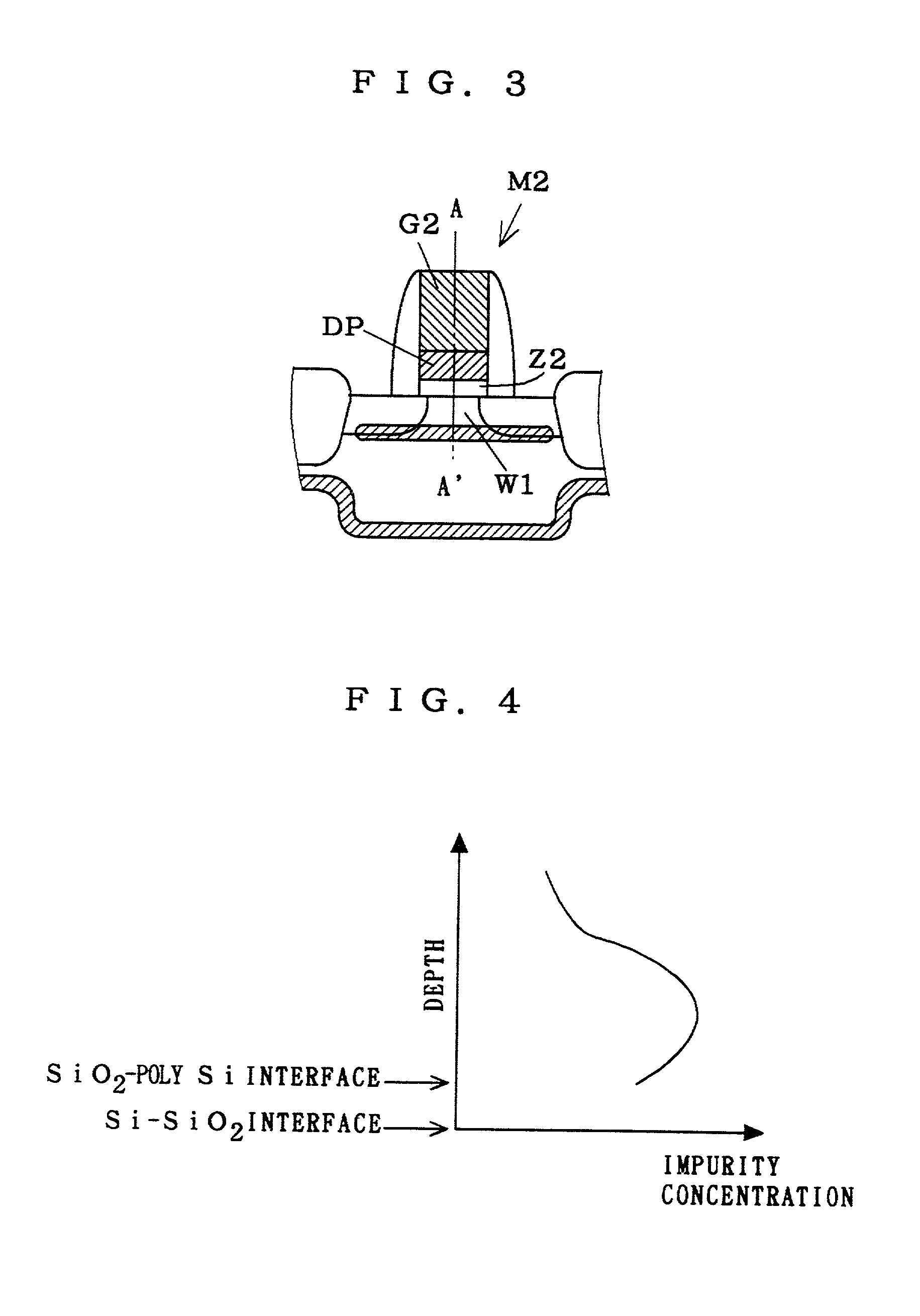
[0256] Roughly speaking, there are two methods to form an electrode which is dsped with an impurity. One method is to form a gate electrode by stacking a doped polysilicon layer. In other words, a stacking material of polysilicon and material gas of an impurity are flown at the same time by a CVD method, so as to dope with an impurity concurrently with formation of a polysilicon layer. With this method, it is possible to keep an impurity profile constant within the polysilicon. FIG. 1 shows a structure of a MOS trans...


PUM


Abstract

According to a semiconductor device and a method of manufacturing the same, a trade-off relationship between threshold values and a diffusion layer leak is eliminated and it is not necessary to form gate oxide films at more than one stages. Since impurity dose are different from each other between gate electrodes (4A to 4C) of N-channel type MOS transistors (T41 to T43), impurity concentration in the gate electrodes (4A to 4C) are different from each other. The impurity concentration in the gate electrodes are progressively lower in the order of higher threshold values which are expected.

Description

BACKGROUND OF THE INVENTION[0001] 1. Field of the Invention[0002] The present invention relates to a semiconductor device and a method of manufacturing the same, and more particularly, to a semiconductor device in which a plurality of types of transistors are formed within one chip and a method of manufacturing such a semiconductor device.[0003] 2. Description of the Background Art[0004] As a semiconductor device in which a plurality of types of transistors (e.g., transistors having different required specifications from each other) are formed within one chip, the following four conventional examples will be described.[0005] <First Conventional Example>[0006] <Overall Structure of DRAM>[0007] First, as a first conventional example, a structure of a DRAM 600 in which a plurality of types of transistors are formed and a method of manufacturing the same will be described. The structure of the DRAM 600 (i.e., cell structure) is shown in FIG. 66.[0008] The DRAM 600 includes n...

Claims


Application Information

Patent Timeline
IPC IPC(8): H01L21/8234H01L21/8242H01L21/8247H01L27/088H01L27/10H01L27/105H01L27/108H01L27/115H01L29/788H01L29/792
CPCH01L27/105H01L27/11526H01L27/11546H10B41/40H10B41/49H01L29/78
Inventor UENO, SHUICHIOKUMURA, YOSHINORIMAEDA, SHIGENOBUMAEGAWA, SHIGETO
Owner RENESAS ELECTRONICS CORP
Learn More