Display device and electronic unit

Active Publication Date: 2010-11-18
JAPAN DISPLAY INC
View PDF5 Cites 97 Cited by
  • Summary
  • Abstract
  • Description
  • Claims
  • Application Information

AI Technical Summary

Benefits of technology

[0074]Now, the operation and effect of the display device 1 will be described.
[0075]In the display device 1, a display driver (not illustrated in the figure) of the pixel substrate 2 line-sequentially supplies the common drive signal Vcom to each of the electrode patterns (such as the common electrodes 431 through 436) in the common electrode 43. The display driver also supplies the pixel signal (image signal) to the pixel electrode 22 through the source line, and line-sequentially controls switching of the TFT in each of the pixel electrodes through the gate line, in synchronization with this supply of the pixel signal. Thereby, the electric field is applied to the liquid crystal layer 6 for each pixel, in the longitudinal direction (direction perpendicular to the substrate) defined by the common drive signal Vcom and each of the pixel signals, and the liquid crystal state is modulated. In this manner, the display is performed with so-called inversion driving.
[0076]On the other hand, on the opposed substrate 4 side, the capacitor element C1 (the capacitor elements C11 through C16) is formed at each intersection portion of each of the electrode patterns in the common electrode 43 and each of the electrode patterns in the detection-electrode-for-sensor 44. Here, for example, as illustrated in Part (A) through Part (C) of FIG. 7, when the common drive signal Vcom is time-divisionally sequentially applied to each of the electrode patterns in the common electrode 43, the charge/discharge is performed on each of the capacitor elements C11 through C16 of one line formed at the intersection portion of the electrode pattern in the common electrode 43, to which the common drive signal Vcom is applied, and each of the electrode patterns in the detection-electrode-for-sensor 44. As a result, the detection signal Vdet with the magnitude in accordance with the capacity of the capacitor element C1 is output from each of the electrode patterns in the detection-electrode-for-sensor 44. In a state in which the user's finger is not in contact with the surface of the opposed substrate 4, the magnitude of this detection signal Vdet is approximately constant. A line of the capacitor elements C1 to be charged/discharged is line-sequentially shifted by the scanning with the common drive signal Vcom.
[0077]Incidentally, when each of the electrode patterns in the com

Problems solved by technology

Therefore, unlike application to stationary television receivers supplied with external power from outlets or the like, it is practically difficult to apply the liquid crystal display element with the touch panel to mobile devices.
Moreover, in the technique described above, it is necessary to bring the conductive film for the touch panel extremely close to the user's finger and therefore, an area where the conductive film for the touch panel is to be disposed is restricted; for instance, it is difficult to dispose the conductive film for the touch panel in, for example, a portion deep inside the liquid crystal display element.
In other words, flexibility in design is low.
Moreover, in the technique described above, it

Method used


Image

  • Display device and electronic unit
  • Display device and electronic unit
  • Display device and electronic unit

Examples


first embodiment

1. First Embodiment

Configurational Example of a Display Device 1

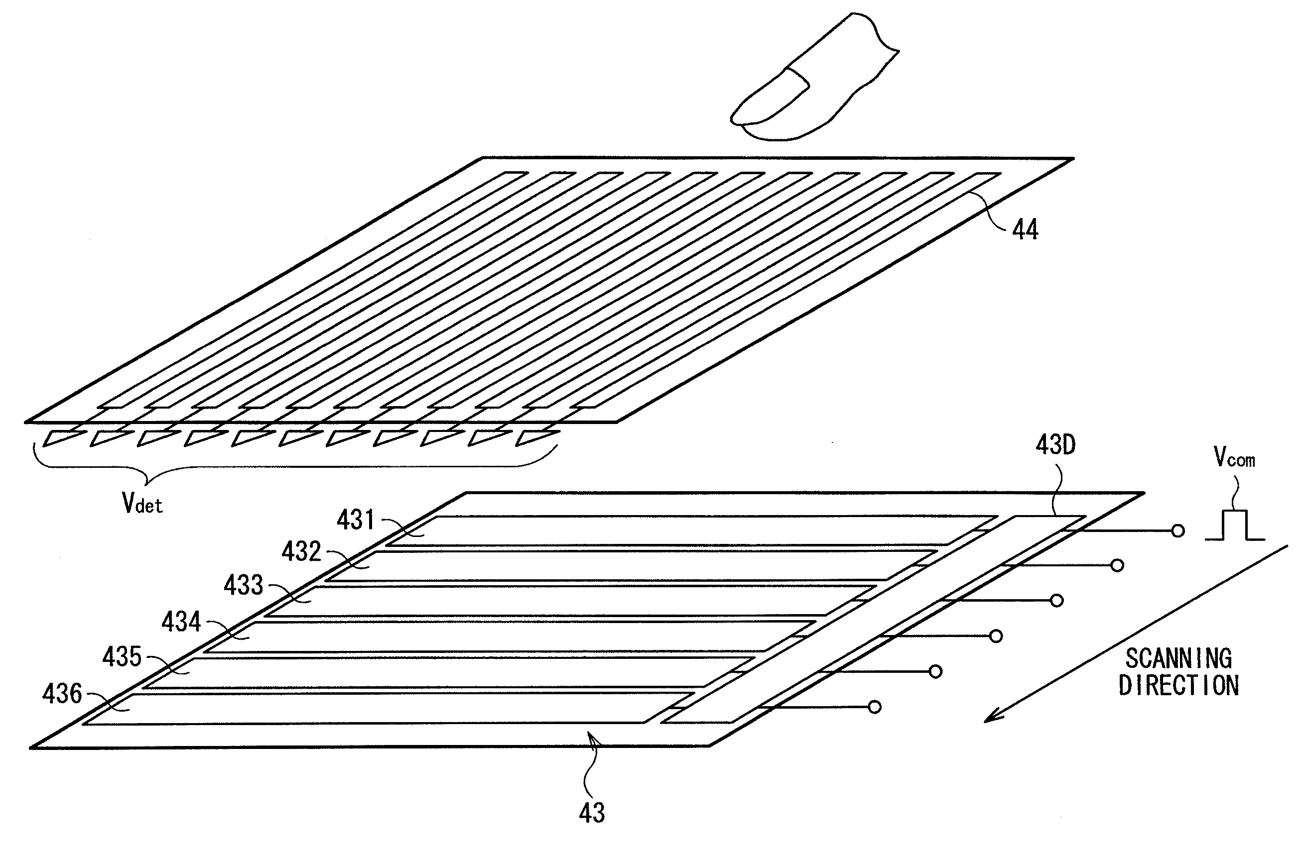
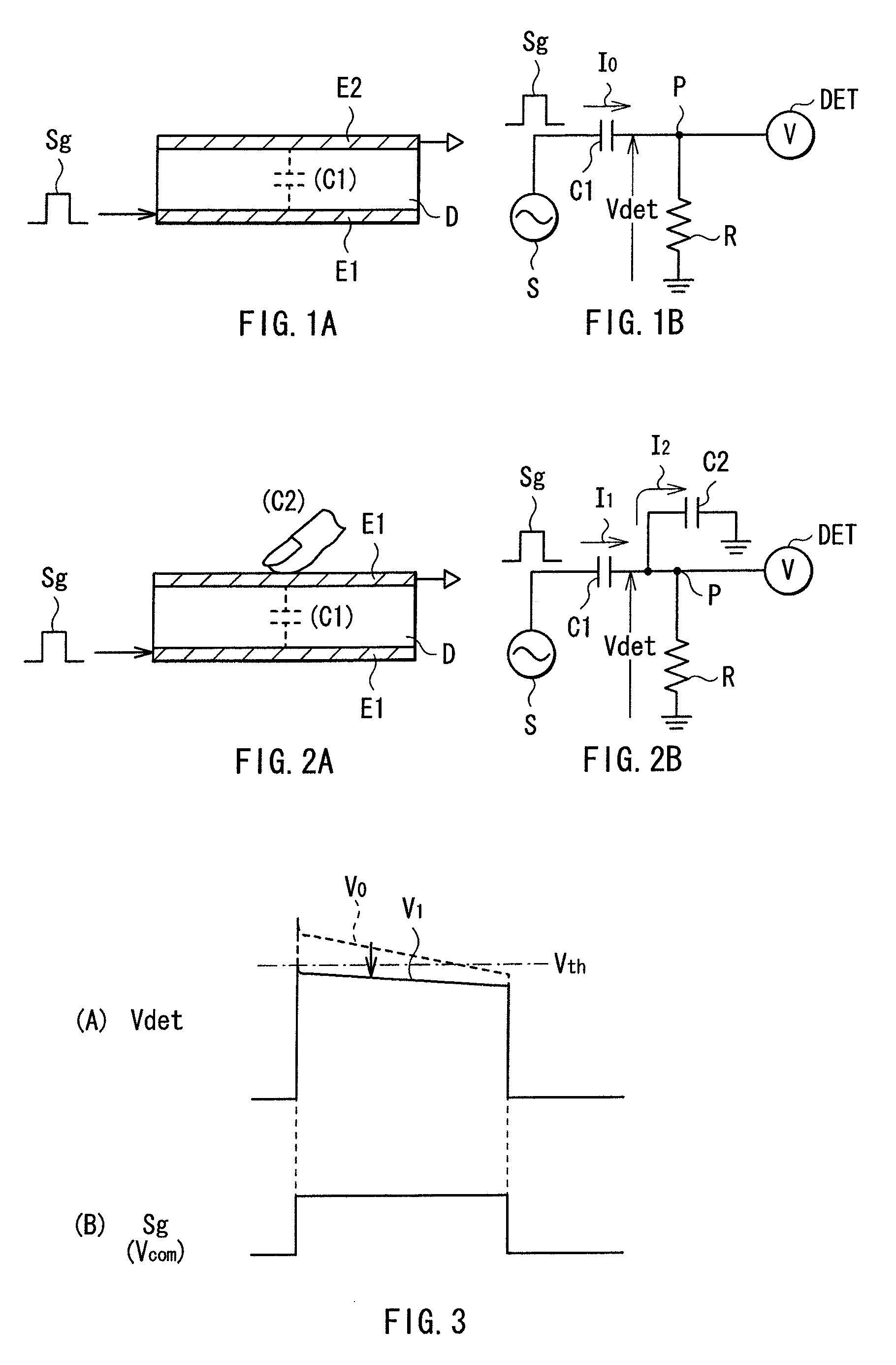
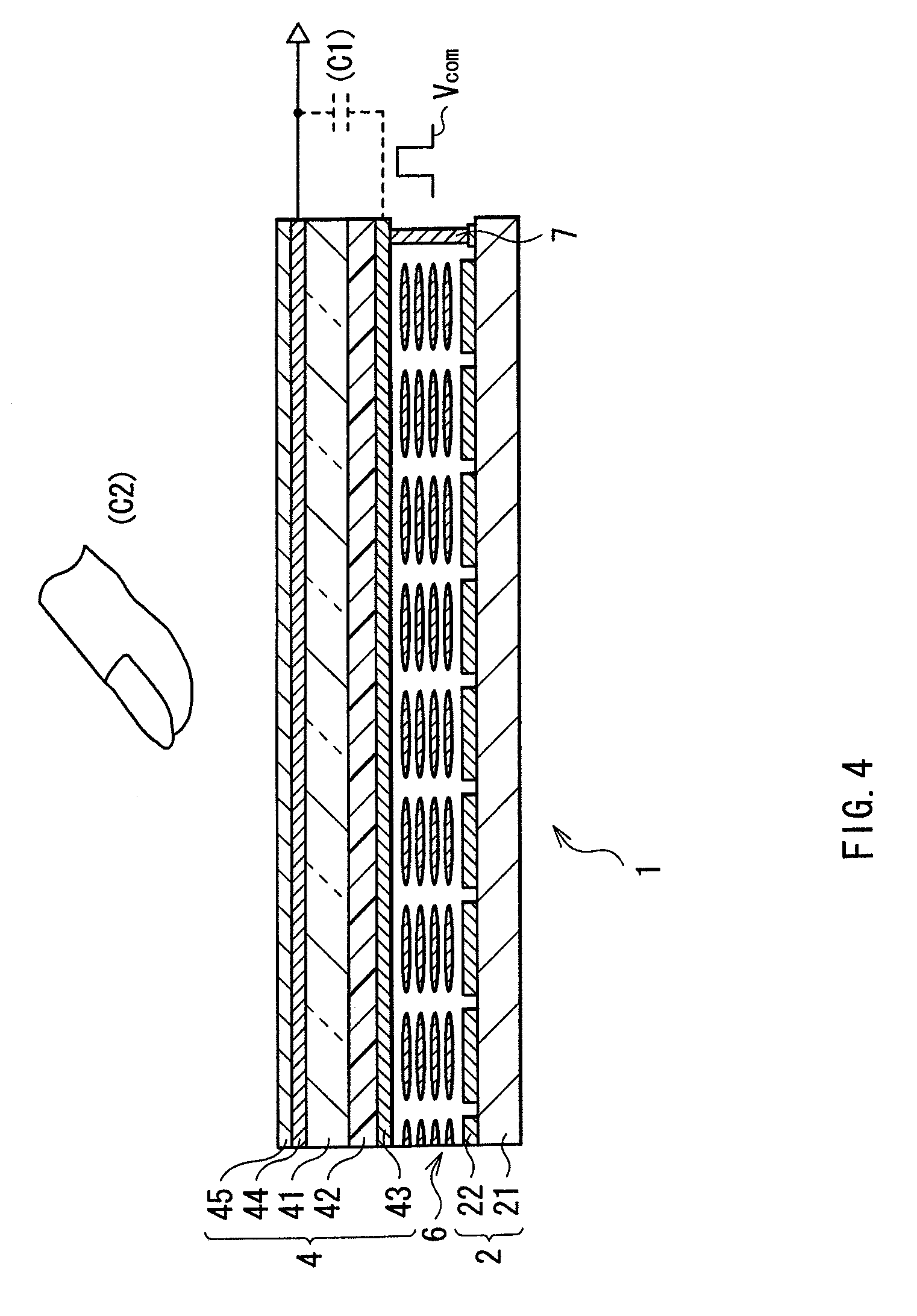
[0056]FIG. 4 illustrates a cross sectional configuration of a main part of the display device 1 with a touch sensor according to a first embodiment of the present invention. In the display device 1, a liquid crystal display element is used as a display element, a part of an electrode (a common electrode 43, which will be described later) that is originally provided in this liquid crystal display element and a drive signal for display (common drive signal Vcom, which will be described later) are used, thereby a capacitance type touch sensor is configured.

[0057]As illustrated in FIG. 4, the display device 1 includes a pixel substrate 2, an opposed substrate 4 facing the pixel substrate 2, and a liquid crystal layer 6 inserted between the pixel substrate 2 and the opposed substrate 4.

[0058]The pixel substrate 2 includes a TFT (thin film transistor) substrate 21 serving as a circuit substrate and a plurality of pixel electr...

second embodiment

2. Second Embodiment

[0095]Next, a second embodiment of the present invention will be described. The second embodiment differs from the above-described first embodiment in that a liquid crystal element in a lateral-electric-field mode is used as a display device.

[Example of the Configuration of a Display Device 1B]

[0096]FIG. 16 illustrates a cross-sectional configuration of a main part of the display device 1B with a touch sensor according to the present embodiment. FIGS. 17A and 17B illustrate details on the configuration of a pixel substrate (pixel substrate 2B that will be described later) in the display device 1B. FIG. 17A is a cross sectional view of the configuration, while 17B is a plan view of the configuration. FIGS. 18A and 18B schematically illustrate the perspective configuration of the display device 1B. Incidentally, in these figures, the elements identical to those of the first embodiment are indicated by the same reference characters as those of the first embodiment, ...

modification 1

(Modification 1)

[0119]FIG. 22 is a perspective diagram that illustrates the configuration of a main part (common electrode and detection-electrode-for-sensor) of a display device with a touch sensor according to Modification 1. As illustrated in FIG. 22, the common electrode 43 may be formed as a single solid electrode, and at the same time, the detection-electrode-for-sensor 44 may be formed as a plurality of individual electrodes arranged in a matrix form. In this case, it is possible to immediately identify a touched position based on the detection signal Vdet from each of the individual electrodes configuring the detection-electrode-for-sensor 44.


PUM


Abstract

The display device with high detection accuracy includes: display pixel electrodes; a common electrode; a display function layer; a display control circuit performing image display control by applying a pixel voltage to each of the display pixel electrodes and applying a common drive voltage to the common electrode, the common drive voltage inverting in synchronization with a drive cycle of the image display control; a touch detection electrode cooperating with the common electrode to form a capacitor; and a touch detection circuit detecting an external proximity object, based on a detection signal obtained from the touch detection electrode in response to the common drive voltage applied to the common electrode. The touch detection circuit performs the detection operation in a inversion period following an inversion timing of the common drive voltage, based on both first and second detection signals obtained before and after the inversion timing, respectively.

Description

[0001]The present application claims priority to Japanese Patent Application JP 2009-120222 filed in the Japanese Patent Office on May 18, 2009, the entire content of which is hereby incorporated by reference.BACKGROUND OF THE INVENTION[0002]1. Field of the Invention[0003]The present invention relates to a display device such as a liquid crystal display device, and particularly relates to a display device which includes a capacitance type touch sensor and into which information can be input with a touch by a user's finger or the like, and to an electronic unit having such a display device.[0004]2. Description of the Related Art[0005]In recent years, attention has been given to a display unit in which a contact detection device (hereinafter, referred to as a touch sensor) generally called a touch panel is directly mounted on a liquid crystal display device and causes the liquid crystal display device to display various buttons for input of information in stead of providing typical bu...

Claims


Application Information

Patent Timeline
IPC IPC(8): G06F3/041
CPCG02F1/13338G06F3/0412G09G3/3648G09G3/3614G06F3/044G06F3/0445G06F3/0446G06F2203/04107G06F3/0448
Inventor NOGUCHI, KOUJIISHIZAKI, KOJINAKANISHI, TAKAYUKITAKEUCHI, TAKEYATERANISHI, YASUYUKI
Owner JAPAN DISPLAY INC
Why Eureka
Try Eureka