Display device and driving method thereof

a display device and driving method technology, applied in the direction of instruments, static indicating devices, etc., can solve the problems of increasing production costs, deterioration of threshold voltage of amorphous silicon thin film transistors, and difficulty in obtaining a wide screen, so as to prevent the transition of a threshold voltage, simplify the pixel circuit, and increase the aspect ratio of pixels

Inactive Publication Date: 2007-02-08
SAMSUNG ELECTRONICS CO LTD
View PDF13 Cites 23 Cited by
  • Summary
  • Abstract
  • Description
  • Claims
  • Application Information

AI Technical Summary

Benefits of technology

[0010] The present invention provides a display device with a simplified pixel circuit that is capable of increasing aspect ratios of pixels and preventing transition of a threshold voltage of ah amorphous silicon thin film transistor to suppress deterioration in image quality, and a method of driving the display device.

Problems solved by technology

However, manufacturing processes for the polysilicon thin film transistors are complex, thus increasing production costs thereof.
In addition, it is difficult to obtain a wide screen by using the organic light emitting display devices.
However, as the amorphous silicon thin film transistors continuously supply a current to the organic light emitting diodes, the threshold voltage of the amorphous silicon thin film transistors may deteriorate.
Even though the same data voltage is applied, non-uniform current flows through the organic light emitting diodes, thus deteriorating the image quality and possibly shortening the life cycle of the organic light emitting display device.

Method used


Image

  • Display device and driving method thereof
  • Display device and driving method thereof
  • Display device and driving method thereof

Examples


Embodiment Construction

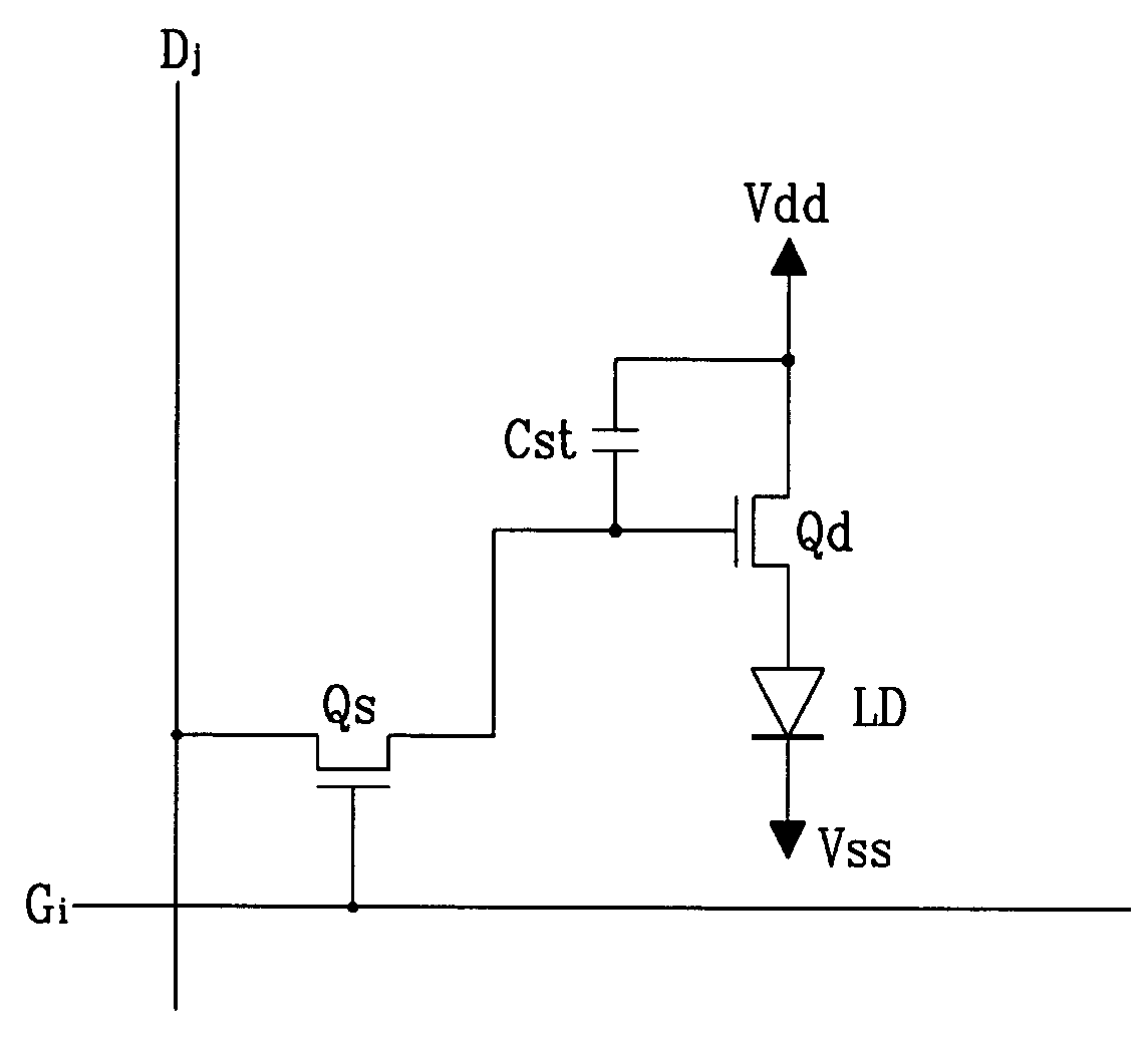
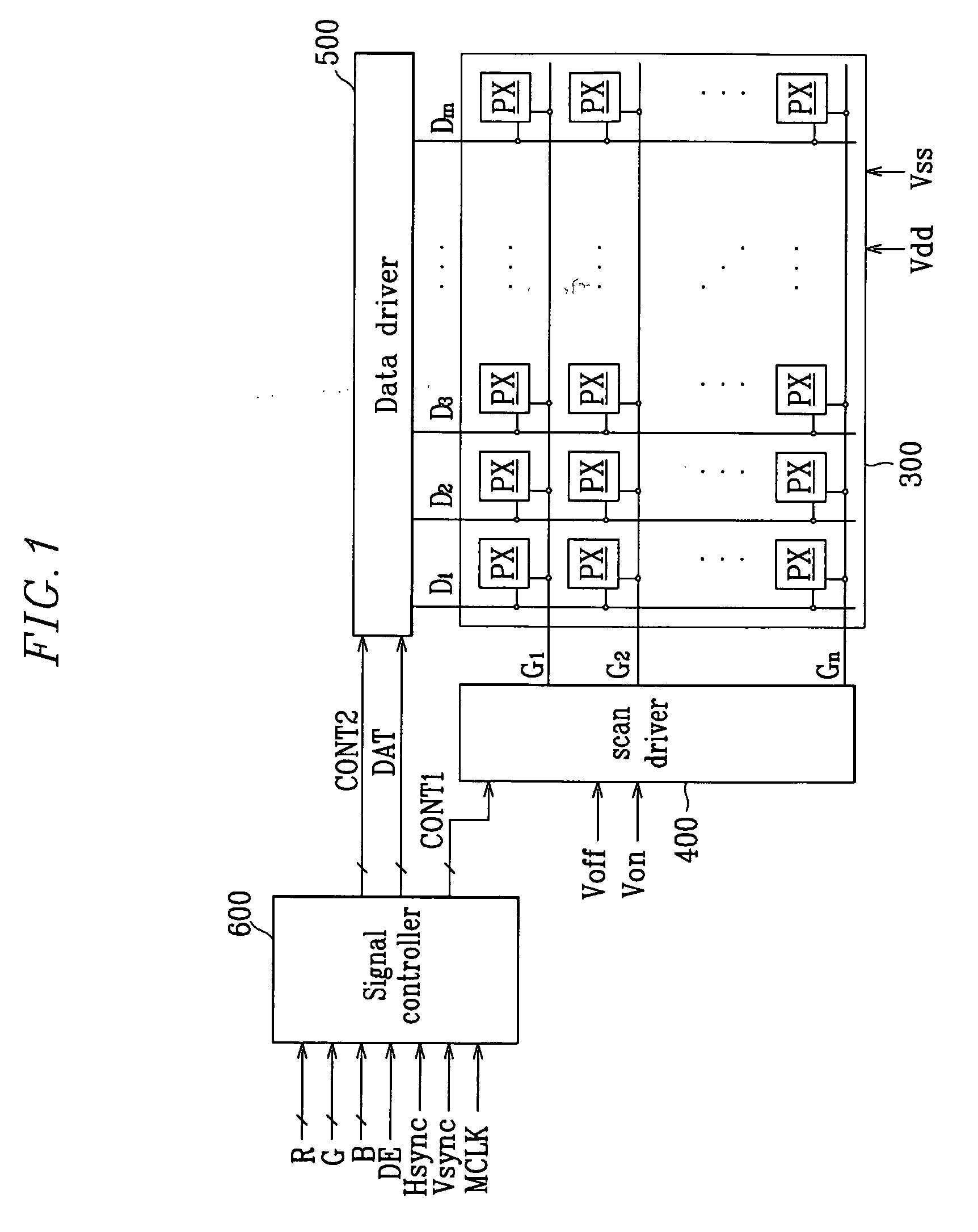
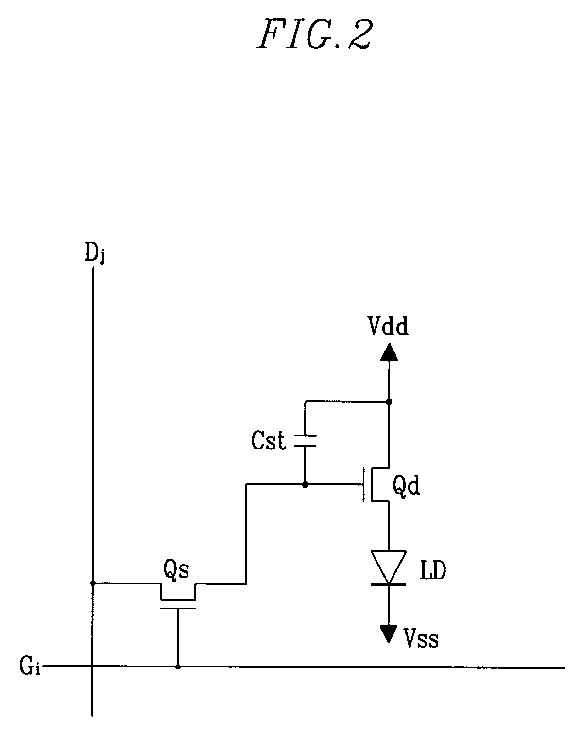
[0046] The invention now will be described more fully hereinafter with reference to the accompanying drawings, in which embodiments of the invention are shown. This invention may, however, be embodied in many different forms and should not be construed as limited to the embodiments set forth herein. Rather, these embodiments are provided so that this disclosure will be thorough and complete, and will fully convey the scope of the invention to those skilled in the art. Like reference numerals refer to like elements throughout.

[0047] It will be understood that when an element is referred to as being “on” another element, it can be directly on the other element or intervening elements may be present therebetween. In contrast, when an element is referred to as being “directly on” another element, there are no intervening elements present. As used herein, the term “and / or” includes any and all combinations of one or more of the associated listed items.

[0048] It will be understood that,...


PUM


Abstract

A display device and a method of driving the display device include first and second pixel row groups having at least one pixel row including a plurality of pixels, a plurality of scan lines, a plurality of data lines, and a data driver generating the data voltage including a normal data voltage and a reverse bias voltage. The data driver applies one of the normal data voltage and the reverse bias voltage to the data line according to a selection signal. The normal data voltage is applied to the driving transistors of the first pixel row group, and the reverse bias voltage is applied to the driving transistors of the second pixel row group. Accordingly, the reverse bias voltages are applied to the pixels, preventing transition of threshold voltages of the driving transistors.

Description

[0001] This application claims priority to Korean Patent Application No. 10-2005-0037604, filed on May 4, 2005, and all the benefits accruing therefrom under 35 U.S.C. §119, and the contents of which in its entirety are herein incorporated by reference. BACKGROUND OF THE INVENTION [0002] (a) Field of the Invention [0003] The present invention relates to a display device and a driving method thereof, and more particularly, to an organic light emitting display device and a driving method thereof. [0004] (b) Description of the Related Art [0005] Recently, as thin and lightweight types of personal computers and television sets have been required, cathode ray tubes (“CRTs”) have been replaced with flat display devices. [0006] Flat display devices include liquid crystal display (“LCD”) devices, field emission display (“FED”) devices, organic light emitting display (“OLED”) devices, plasma display panel (“PDP”) devices, and the like. [0007] The organic light emitting display device include...

Claims


Application Information

Patent Timeline
Patent Type & Authority Applications(United States)
IPC IPC(8): G09G3/30
CPCG09G3/3233G09G2300/0465G09G2300/0819G09G2300/0842G09G2320/043G09G2310/0254G09G2310/04G09G2320/0261G09G2310/0221G09G3/20G09G3/30
Inventor PARK, KYONG-TAESUNG, SI-DUKKIM, NAM-DEOG
Owner SAMSUNG ELECTRONICS CO LTD
Why Eureka
Try Eureka