Liquid crystal display device and electronic apparatus

a display device and liquid crystal technology, applied in non-linear optics, instruments, optics, etc., can solve the problems of increased defects and low image quality, and achieve the effects of suppressing image quality degradation, high display quality, and improving viewing angl

Active Publication Date: 2007-04-19
SEMICON ENERGY LAB CO LTD
View PDF17 Cites 23 Cited by
  • Summary
  • Abstract
  • Description
  • Claims
  • Application Information

AI Technical Summary

Benefits of technology

[0043] Orientation of a liquid crystal can be controlled by providing a cell gap adjusting film in a reflection region of a pixel electrode, and providing a step portion thereof (a boundary portion of the cell gap adjusting film) so as to overlap in parallel with a slit portion at a boundary portion between a reflection region and a transmission region. Therefore, a semi-transmission type liquid crystal display device with high display quality can be obtained by improving a viewing angle when displaying an image and by suppressing deterioration of image quality due to disorder of orientation of the liquid crystal.

Problems solved by technology

However, there are a number of places where directions of orientation of liquid crystals are different; there are problems that orientation control of a liquid crystal is difficult, a defect such as a disclination easily occurs, and image quality becomes low.
In particular, in the case of a pixel structure combining a reflecting electrode with a transparent electrode such as a conventional semi-transmission type liquid crystal display device, there is a problem that these defects are increased.

Method used


Image

  • Liquid crystal display device and electronic apparatus
  • Liquid crystal display device and electronic apparatus
  • Liquid crystal display device and electronic apparatus

Examples


embodiment mode 1

[Embodiment Mode 1]

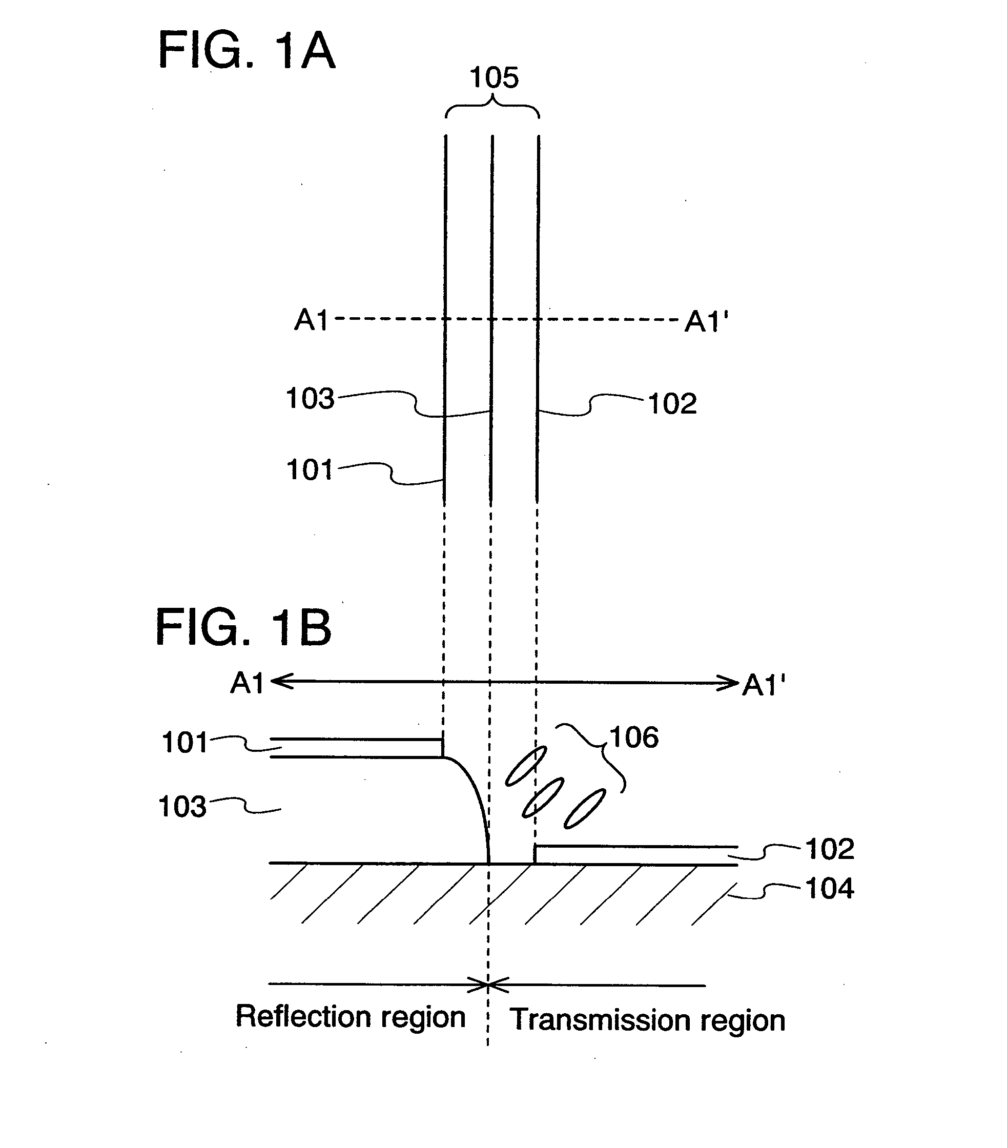
[0094] In this embodiment mode, description is made of a structure of a semi-transmission type liquid crystal (which includes a reflection region and a transmission region in one pixel, and can be employed both as a transmission type liquid crystal and a reflection type liquid crystal) employing a vertically aligned liquid crystal, which has different cell gaps (a distance between two electrodes arranged to face each other through a liquid crystal) of a liquid crystal in the transmission region and the reflection region, so that a display can be performed normally. A light entering a liquid crystal is passed through the liquid crystal twice in the reflection region, and a light is passed through the liquid crystal once in the transmission region. Therefore, it is required to perform a similar display in the case of performing a display as the transmission type liquid crystal and in the case of performing a display as the reflection type liquid crystal, and a cell ...

embodiment mode 2

[Embodiment Mode 2]

[0119] This embodiment mode describes an example other than the case where the reflection electrode 101 is formed over the cell gap adjusting film 103 described in Embodiment mode 1.

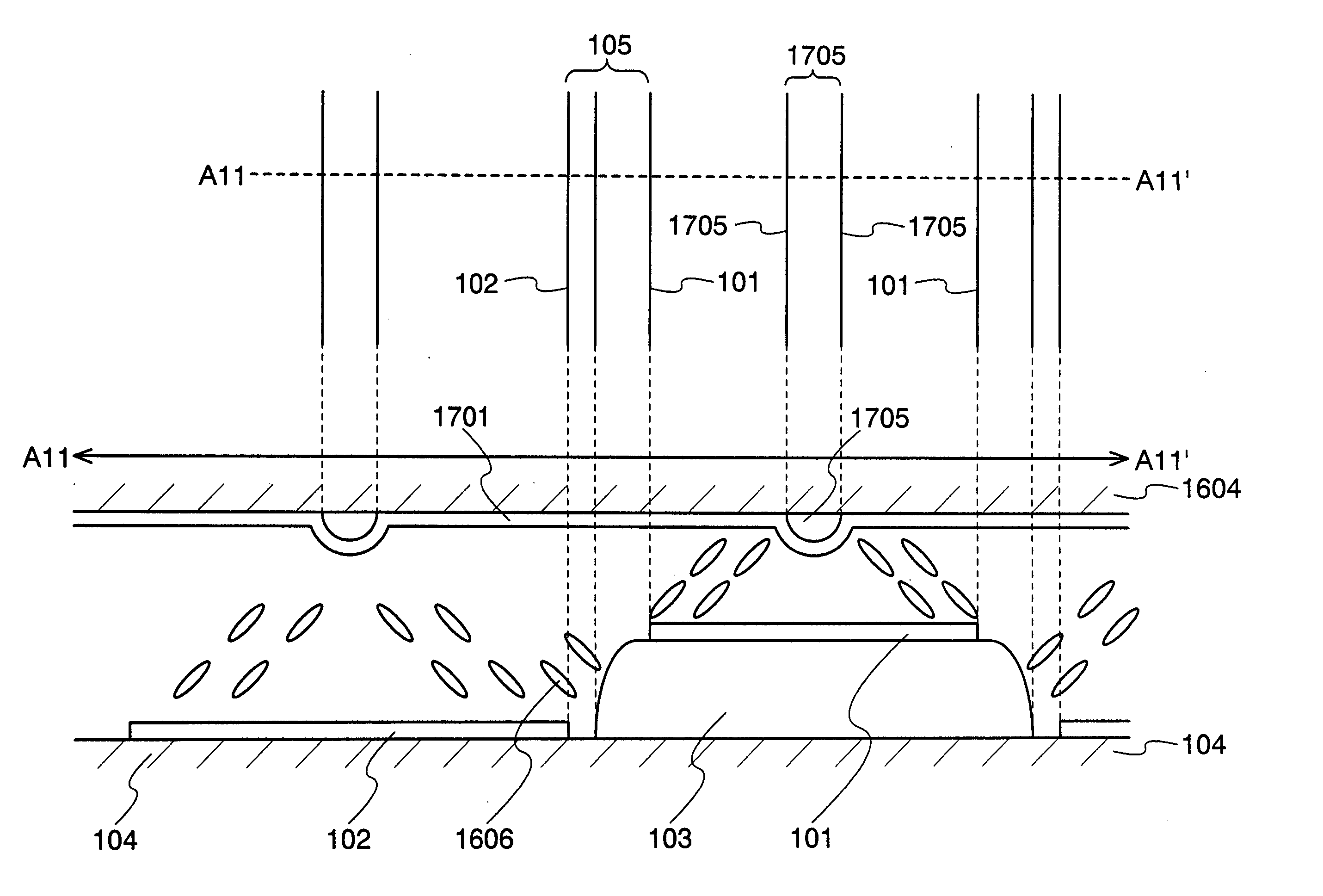
[0120]FIG. 6A is a top plan layout view. FIG. 6B is a cross sectional view of FIG. 6A. As shown in FIG. 6A, in the case where a reflection electrode 601, a transparent electrode 602, a transparent electrode 102, a slit 605 (a gap, a space, or the like) of an electrode are provided, the reflection electrode 601, the transparent electrode 602 and the transparent electrode 102 are arranged approximately in parallel, and the slit 605 (the gap, the space, or the like) of the electrode is also arranged in parallel. A cell gap adjusting film (a boundary portion thereof) 103 is arranged approximately in parallel therewith. The boundary portion of the cell gap adjusting film 103 is provided between the reflection electrode 601 and the transparent electrode 102. As shown in FIG. 6B, the reflect...

embodiment mode 3

[Embodiment Mode 3]

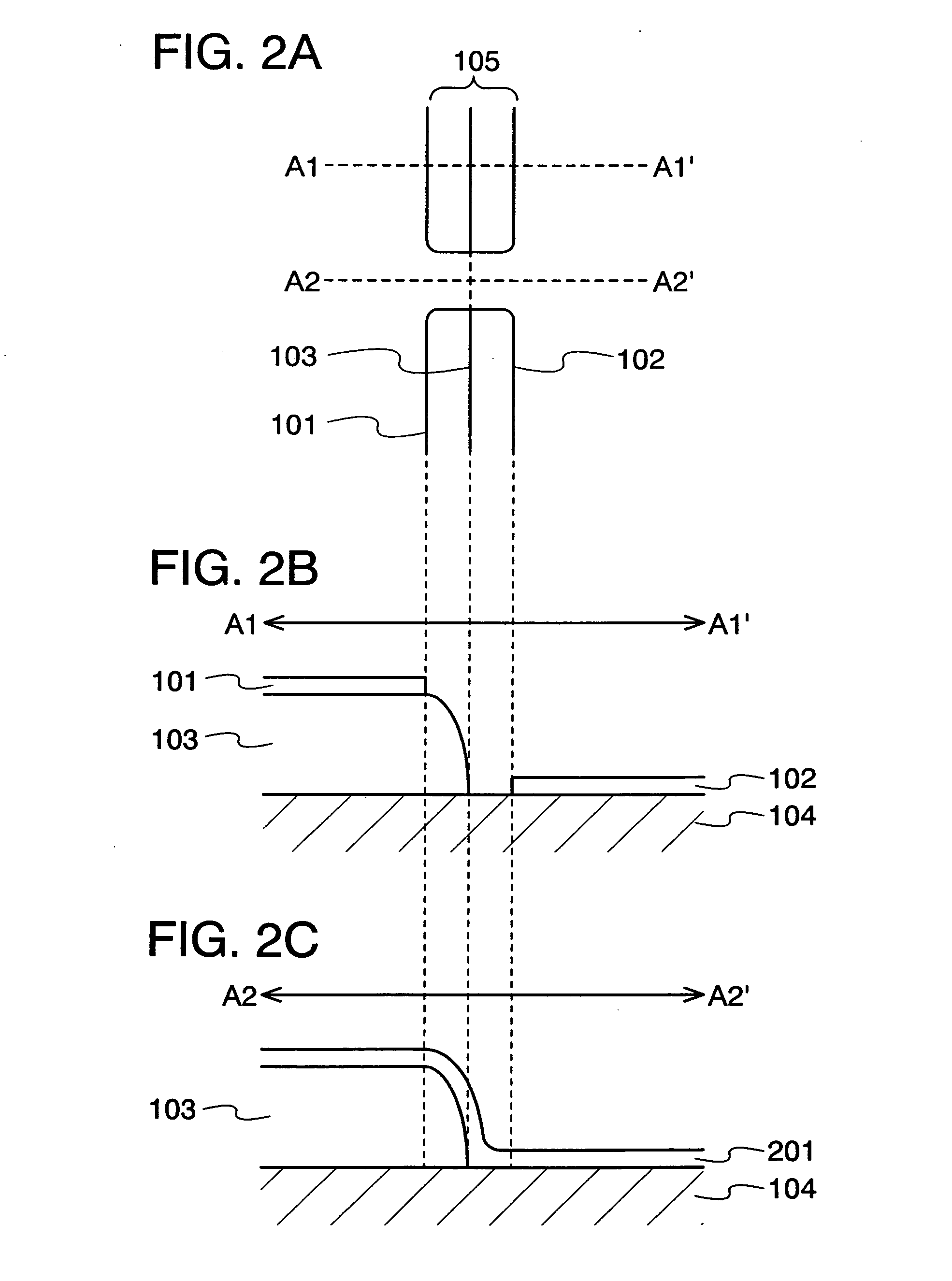
[0128] Although description is made of the case where the reflection electrode is even in Embodiment Modes 1 and 2, it is not limited to this. When the reflection electrode is uneven, light is diffused; therefore, a whole luminance is averaged and a clear image can be obtained in the case of performing a display of reflecting mode.

[0129]FIGS. 7A and 7B show an example of the case where the reflection electrode has an uneven portion. An upper surface of a cell gap adjusting film 703 has an uneven portion. As a result, a reflection electrode 701 which is formed over the cell gap adjusting film 703 has an uneven portion. Note that it is not preferable that the uneven portion be too large because a large uneven portion affects a direction that the liquid crystal is inclined. Therefore, a thickness d4 of a projecting portion of the cell gap adjusting film 703 is preferably smaller than the thickness d3 of the cell gap adjusting film 703. For example, the thickness d4 ...


PUM

PropertyMeasurementUnit
thickness d3aaaaaaaaaa
distance d2aaaaaaaaaa

Abstract

The present invention provides a liquid crystal display device including a liquid crystal layer disposed between a first substrate and a second substrate, a pixel electrode in a reflection region and a transmission region over the first substrate, a film for adjusting a cell gap in the reflection region over the first substrate, and an opposite electrode in the reflection region and the transmission region over the second substrate. The pixel electrode in the reflection region is provided over the film and reflects light. The pixel electrode in the transmission region transmits light. The pixel electrode in the reflection region and the transmission region includes a slit. The slit is overlapped with at least a part of a step portion which is provided by the film between the reflection region and the transmission region.

Description

BACKGROUND OF THE INVENTION [0001] 1. Field of the Invention [0002] The present invention relates to a liquid crystal display device performing a display of reflection type and transmission type, and particularly to a liquid crystal display device performing a display of a multi-domain mode. [0003] 2. Description of the Related Art [0004] A liquid crystal display device is used for various electronic products such as a mobile phone, a monitor of navigation system, and a television. Some of these electronic products are used outside as well as inside, and a semi-transmission type liquid crystal display device is known, which includes both features of a transmission mode and a reflection mode in order to ensure a high visibility both outside and inside. [0005] As for a semi-transmission type liquid crystal display device, a display device is known, which includes a pixel including a liquid crystal sandwiched between an active matrix substrate and an opposite substrate, a reflection po...

Claims


Application Information

Patent Timeline
Patent Type & Authority Applications(United States)
IPC IPC(8): G02F1/1337
CPCG02F1/133371G02F1/133555G02F1/133707G02F2203/09G02F1/1335G02F1/1343G02F1/1337
Inventor KIMURA, HAJIME
Owner SEMICON ENERGY LAB CO LTD
Why Eureka
Try Eureka