Multilayer ceramic board and manufacturing method thereof

a technology of multi-layer ceramics and manufacturing methods, applied in the direction of resistive material coatings, non-metallic protective coating applications, metallic pattern materials, etc., can solve the problems of inferior strength reduced chemical resistance and durability of multi-layer ceramic boards, damaged surfaces or vias,

Inactive Publication Date: 2010-12-02
SAMSUNG ELECTRO MECHANICS CO LTD
View PDF0 Cites 10 Cited by
  • Summary
  • Abstract
  • Description
  • Claims
  • Application Information

AI Technical Summary

Benefits of technology

[0018]The present invention has been invented in order to overcome the above-described problems and it is, therefore, an object of the present invention to pr

Problems solved by technology

In this case, since diffused reflection of lights is generated due to nature of a ceramic material, there has been a problem in performing alignment control required for not only the photo process for forming the contact pads on the multilayer ceramic board, but also the process for forming the probe pins.
However, in case where the pigment was included in the multilayer ceramic board, there has been problems that chemical resistance and durability of the multilayer ceramic board were reduced.
Thus, the multilayer ceramic board had an inferior strength, and damaged surfaces or damaged vias due to chemicals, such as a strong acid or a strong base used in a photo process or an MEMS process for forming contact pads or probe pins.
Furthermore, for example, in case where the probe pins were formed on the

Method used


Image

  • Multilayer ceramic board and manufacturing method thereof
  • Multilayer ceramic board and manufacturing method thereof
  • Multilayer ceramic board and manufacturing method thereof

Examples


first embodiment

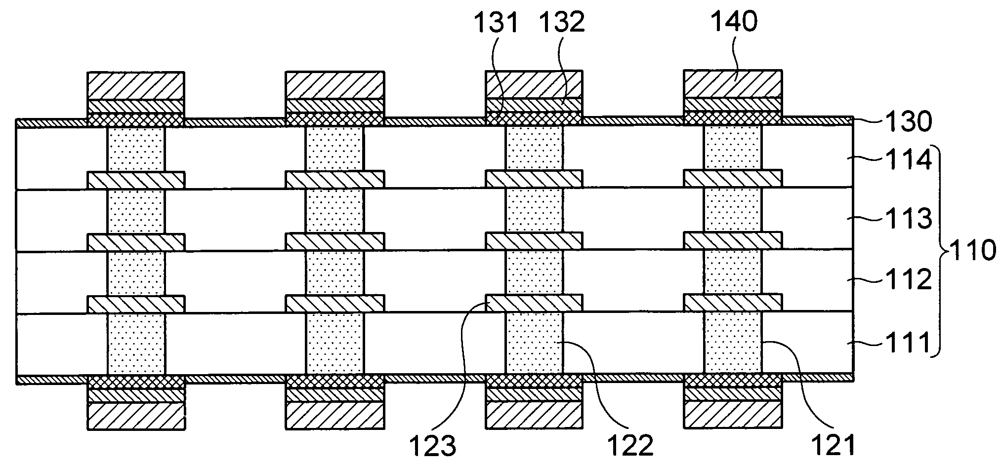
[0042]FIG. 1 is a cross-sectional view of a multilayer ceramic board in accordance with the present invention.

[0043]Referring to FIG. 1, a multilayer ceramic board in accordance with the embodiment of the present invention may include a ceramic stacked structure 110, diffused reflection preventing patterns 130, and contact pads 140.

[0044]The ceramic stacked structure 110 may include ceramic layers 111, 112, 113, and 114 formed by being stacked in multiple layers. In this case, the ceramic layers 111, 112, 113, and 114 formed by being staked in multiple layers are provided with the vias 122 to allow the layers to be connected to one another, wherein the vias include a conductive material filled in via holes 121 which pass through their bodies, for example, an Ag paste. Also, inner circuit patterns 123 electrically connected to the vias 122 are further provided in the ceramic stacked structure 110.

[0045]The diffused reflection preventing patterns 130 expose the vias 122 provided on ea...

second embodiment

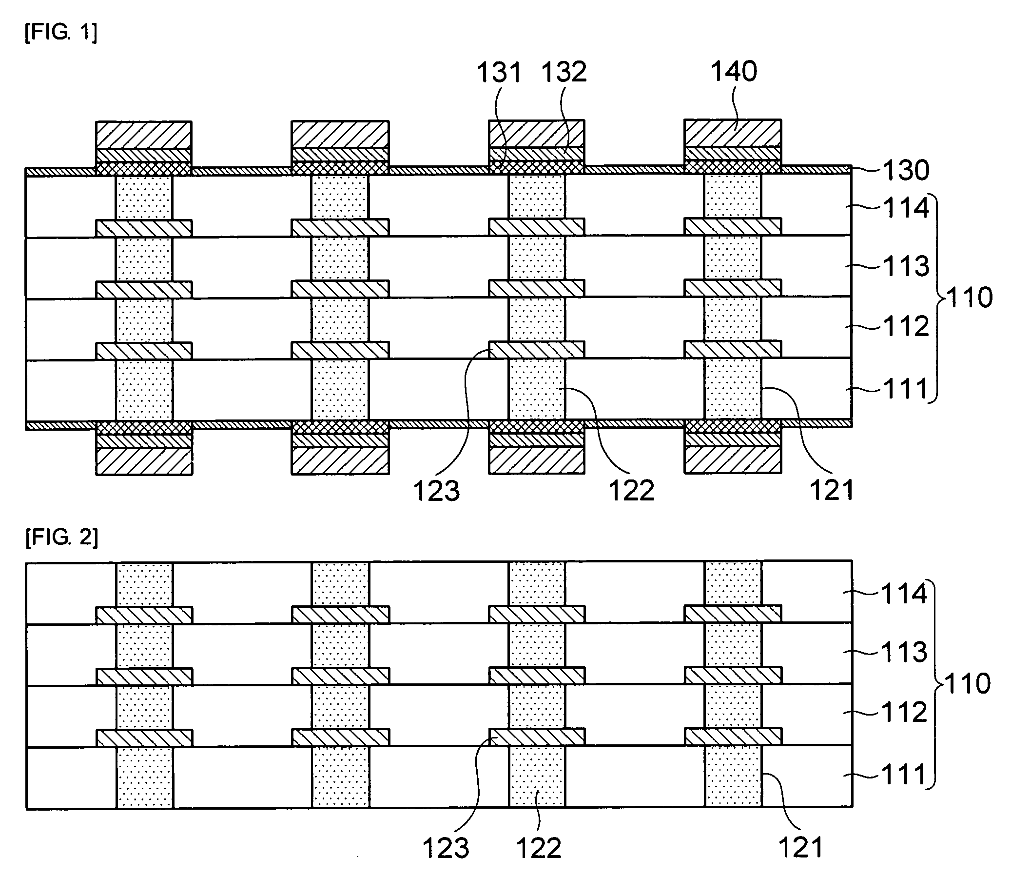
[0059]FIGS. 2 to 9 are cross-sectional views for explaining a method of manufacturing the multilayer ceramic board in accordance with the present invention.

[0060]Referring to FIG. 2, in order to manufacture the multilayer ceramic board, the ceramic stacked structure 110 may be provided in which a plurality of ceramic layers 111, 112, 113, and 114 are stacked and interconnected to one another through the vias 112.

[0061]The ceramic stacked structure 110 may be formed by allowing green sheets having the vias 122 to be stacked in multiple layers and firing the stacked green sheets. In the stacked green sheets, interlayer connection can be achieved through the vias 122. The green sheets further include inner circuit patterns 123 connected to the vias 122.

[0062]Referring to FIG. 3, mask patterns 150 are formed which cover the vias 122 provided on each of the uppermost ceramic layer 114 and the lowermost ceramic layer 111.

[0063]The mask patterns 150 may be formed to correspond to a formati...

third embodiment

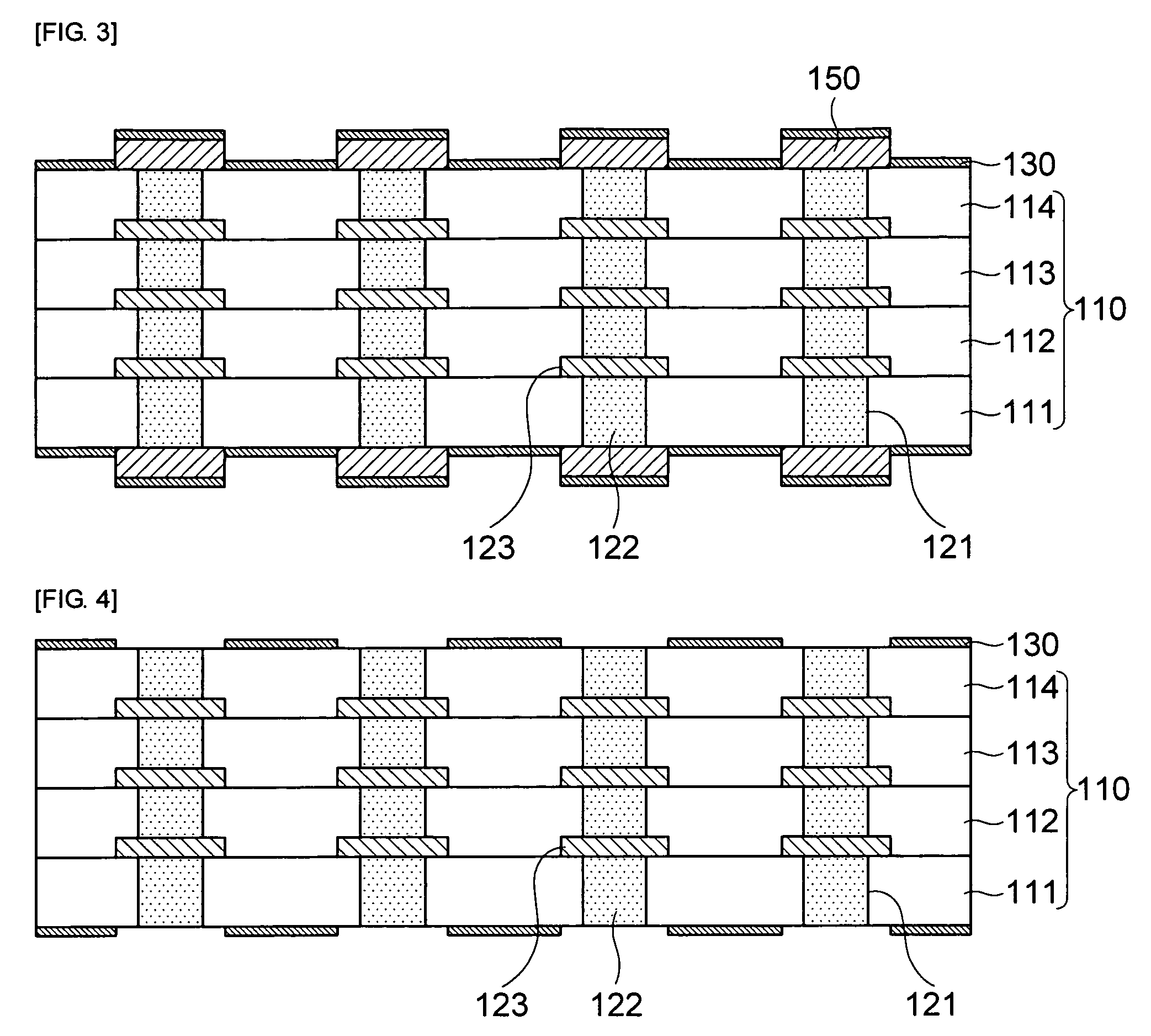
[0080]FIGS. 10 to 12 are cross-sectional views illustrating a method of manufacturing the multilayer ceramic board in accordance with the present invention.

[0081]Referring to FIG. 10, in order to manufacture the multilayer ceramic board, a pre-ceramic stacked structure 110a formed by being staked with a plurality of ceramic layers is first provided. Herein, the interlayer connection is made in the pre-ceramic stacked structure 110a by the vias 122 provided in each of the ceramic layers 112 and 113.

[0082]Thereafter, the green sheets 211 and 214 having the diffused reflection preventing patterns 130 are provided on each of the both sides of the pre-ceramic stacked structure 110a.

[0083]In order to form the diffused reflection preventing patterns 130 on the green sheets 211 and 214, the vias 122 are formed by passing the green sheets 211 and 214. Herein, the inner circuit patterns 123 electrically connected to the vias 122 may be further formed on the green sheets 211 and 214.

[0084]On ...


PUM

PropertyMeasurementUnit
Fracture energyaaaaaaaaaa

Abstract

The present invention relates to a multilayer ceramic board and manufacturing method thereof. The multilayer ceramic board includes: a ceramic stacked structure in which multiple ceramic layers are stacked and interconnected to one another through vias; diffused reflection preventing patterns which expose the vias provided on each of the uppermost ceramic layer and the lowermost ceramic layer, and are disposed on each of a top surface and a bottom surface of the ceramic stacked structure; and contact pads which are electrically connected to the vias exposed by the diffused reflection preventing patterns.

Description

CROSS-REFERENCE TO RELATED APPLICATIONS[0001]This application claims the benefit of Korean Patent Application No. 10-2009-0046954 filed with the Korea Intellectual Property Office on May 28, 2009, the disclosure of which is incorporated herein by reference.BACKGROUND OF THE INVENTION[0002]1. Field of the Invention[0003]The present invention relates to a multilayer ceramic board and manufacturing method thereof; and, more particularly, to a multilayer ceramic board provided with diffused reflection preventing patterns disposed on each of top and bottom surfaces of a ceramic stacked structure.[0004]2. Description of the Related Art[0005]The recent trend toward technical development of electric apparatus and thinness of the apparatus itself causes essential integration of its components.[0006]There has been developed a multilayer ceramic board formed by stacking a number of ceramic sheets for integration of its components. As the multilayer ceramic board has thermal resistance, abrasio...

Claims


Application Information

Patent Timeline
IPC IPC(8): H05K1/09B05D5/12B32B38/00
CPCC04B37/006H05K2203/166C04B2237/365C04B2237/62H05K1/0269H05K1/0306H05K1/113H05K3/108H05K3/28H05K3/388H05K3/4629H05K2201/0112H05K2201/0175H05K2201/0179H05K2201/096H05K2201/09918H05K2203/1383C04B2237/125H05K3/46H05K3/00
Inventor KIM, YONG SUKCHANG, BYEUNG GYUYOO, WON HEEOH, YONG SOO
Owner SAMSUNG ELECTRO MECHANICS CO LTD
Why Eureka
Try Eureka