

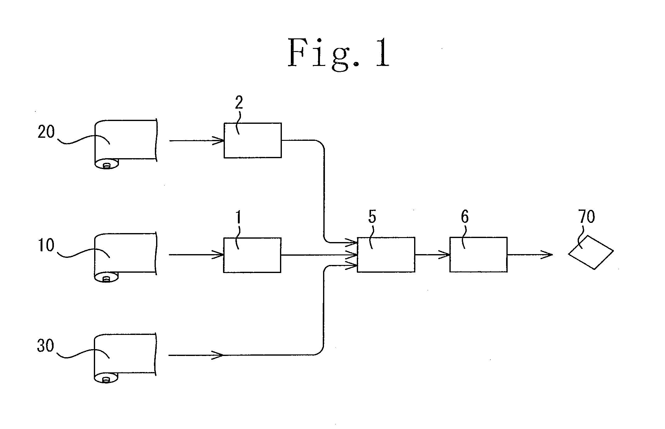
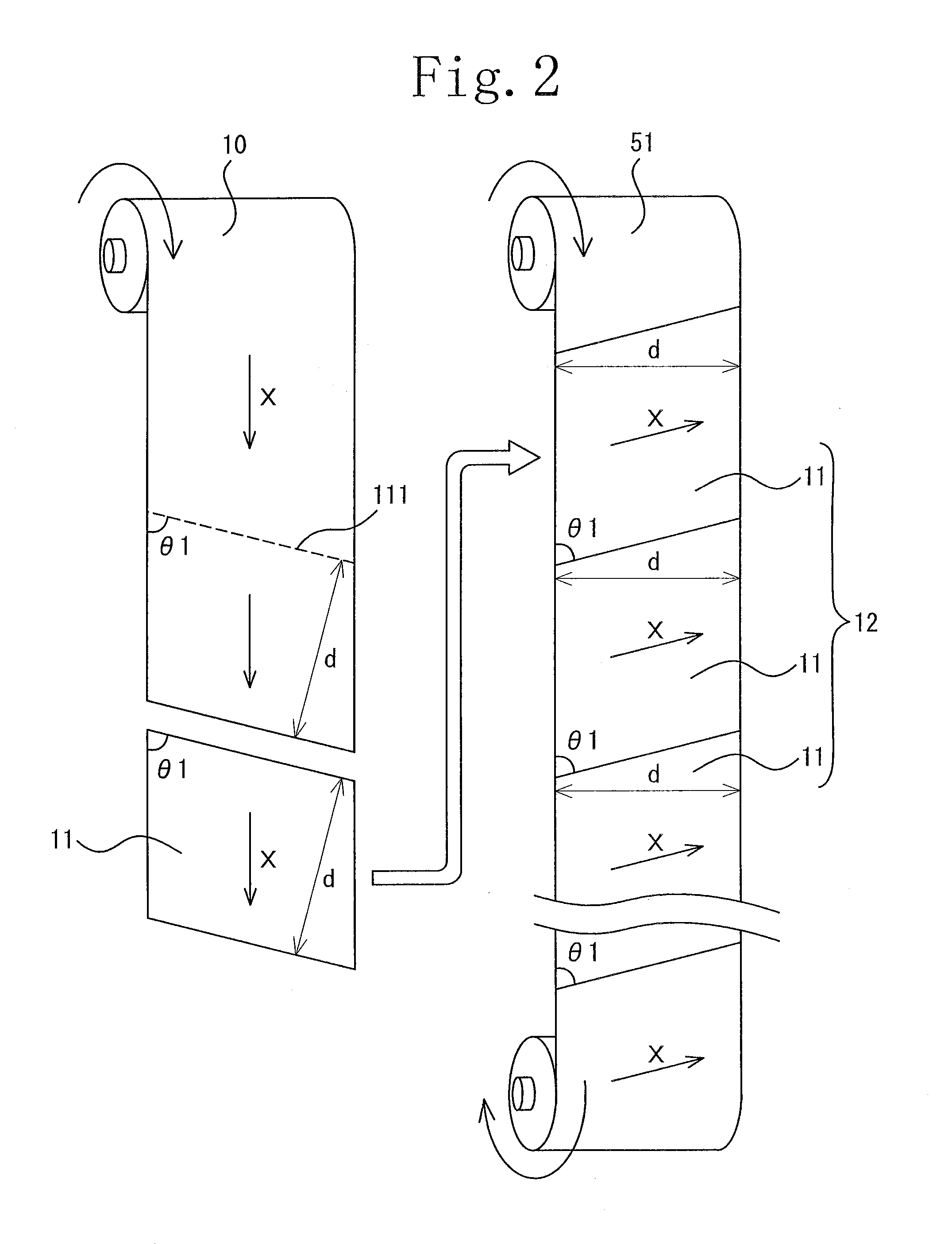
Method of producing optical film laminate
a technology of optical film and cutting film, which is applied in the field of producing optical film laminate, can solve the problems of difficult cutting operation and handling of cut film, and achieve the effect of improving the working property and improving the yield per area of optical film
- Summary
- Abstract
- Description
- Claims
- Application Information
AI Technical Summary
Benefits of technology
Problems solved by technology
Method used
Image

Examples
example 1
Calculation Example 1
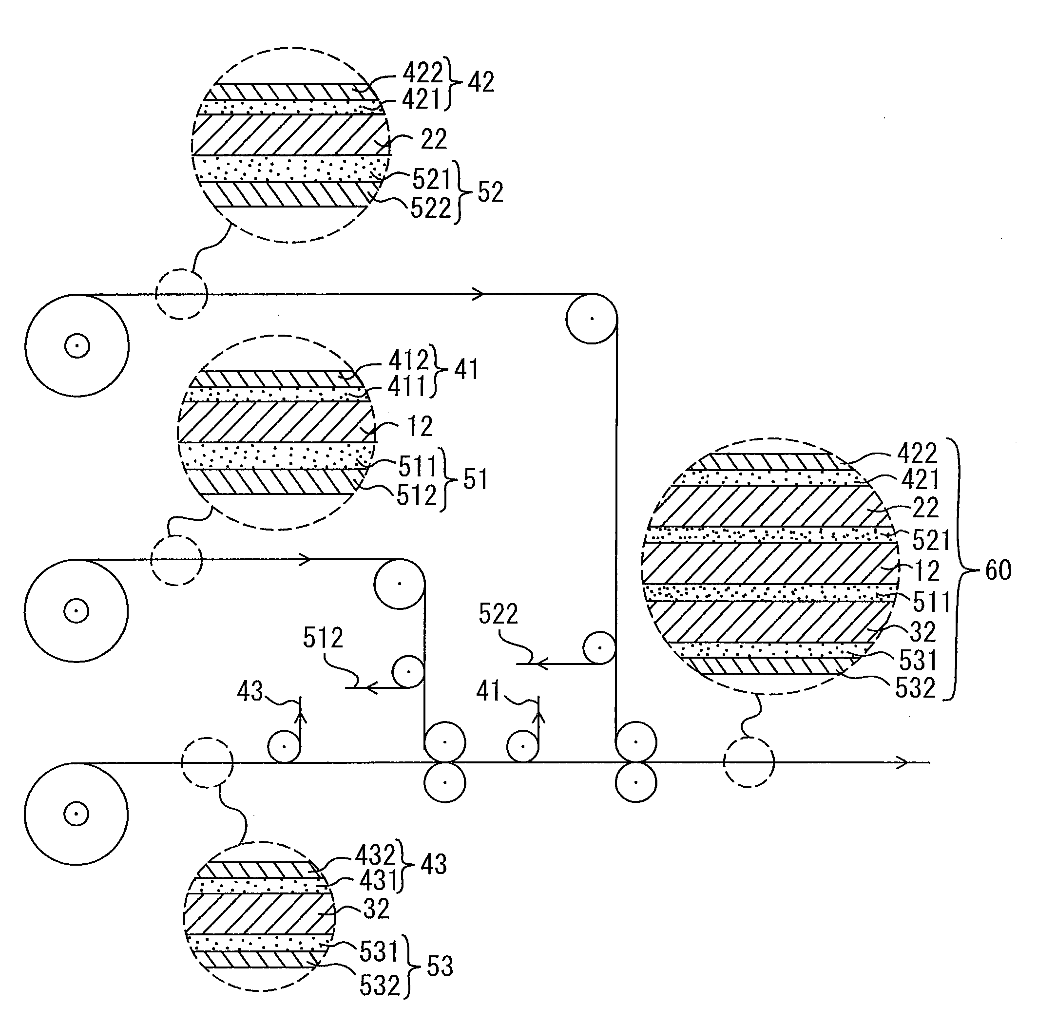
[0082]A retardation film having a width of 1150 mm was used for a first optical film and a second optical film, and a polarizing film having a width of 1180 mm was used for a third optical film. The calculation was made for the case where these are laminated together to form a laminate chip (a three-layer product) having a length of 30 mm and a width of 40 mm.
[0083]The slow axis of the retardation film as the first optical film, the slow axis of the retardation film as the second optical film and the absorption axis of the polarizing film as the third optical film were respectively set at 45°, 105° and 120° relative to the long side of the laminate chip.
[0084]The yield (%) per area of each of the used first to third optical films was calculated and each average value was calculated, which average value was designated as the yield of each method. The result is shown in Table 1.
TABLE 1First opticalSecond opticalThird opticalAveragefilmfilmfilmvalueExample 1-182.2%...
example 2
Calculation Example 2
[0085]A retardation film having a width of 820 mm, a retardation film having a width of 1090 mm and a retardation film having a width of 1250 mm were used respectively for first to third optical films, and a polarizing film having a width of 1185 mm was used for a fourth optical film. The calculation was made for the case where these are laminated together to form a laminate chip (a four-layer product) having a length of 30 mm and a width of 40 mm.
[0086]The slow axis of the retardation film as the first optical film, the slow axis of the retardation film as the second optical film, the slow axis of the retardation film as the third optical film and the absorption axis of the polarizing film as the fourth optical film were respectively set at 45°, 105°, 120° and 30° relative to the long side of the laminate chip.
[0087]The yield (%) per area of each of the used first to fourth optical films was calculated and each average value was calculated, which average value ...
PUM
| Property | Measurement | Unit |
|---|---|---|
| Angle | aaaaa | aaaaa |
| Angle | aaaaa | aaaaa |
| Fraction | aaaaa | aaaaa |
Abstract
Description
Claims
Application Information